PCB是我们生活中常见的电路产品,在电子设计行业中,嵌入式产品的最终文件也是PCB文件。
一个PCB项目一般包含四个文件:xxx.SchDoc(PCB原理图)、xxx.PcbDoc(PCB封装图)、xxx.SchLib(PCB原理图库)、xxx.PcbLib(PCB封装库)。
大致流程是:先绘制[PCB原理图库SchLib],再绘制[PCB封装库PcbLib],并将原理图库元器件与封装库进行关联。
然后画出[PCB原理图SchDoc],更新为[PCB封装图PcbDoc],Design->update PCB Document,最后布局覆铜。
Why use Gerber? Gerber, also known as image files, is a standard file format. Gerber consists of two important parts, the Gerber image file is used to describe the content of a certain layer (somewhat similar to film), and the NC drilling file.
PCB manufacturers can directly produce the final PCB through Gerber, and the commonly used format is RS-274X. Most board manufacturers also support the latest Gerber X2 format (which includes more board stacking information and attributes). Many engineers like to directly send PCB design files to the board factory, but this "lazy" approach is actually risky because the board factory still needs to convert the PCB file into Gerber before production, so there are many potential problems in the process from PCB to Gerber.
Due to issues with the EDA tool version, the PCB files opened by the board factory may have been altered.
Due to a lack of communication, some parameters that do not need to be displayed on the PCB remain on the finished product.
In short, the process of converting PCB to Gerber may not be the same as copying, and designers should be responsible for this process. So most experienced engineers manually convert PCBs into Gerber, and then use software such as CAM350 to check if there are any issues with the Gerber before sending it to the board factory for processing. In addition, whether you use Altium, Allegro, or Expedition, as long as you convert to Gerber, the board factory can recognize it correctly. Another point is that Gerber finds it difficult to generate PCBs in reverse, and for safety reasons, companies are also unwilling to directly send the design source files to the board factory.
PCB gerber files typically include outlines, CNC (electroplated and non electroplated), screen printed layers, solder mask layers, copper layers, and solder paste layers.
The layout file consists of D-code and coordinate files. Without D-code, the routing will have no width, and the solder pads will only have contours; If there are no coordinates, there will be no graphic outline and board size; Usually, coordinate files reflect layout files, while D-code files sometimes exist separately. In this case, we need to identify these D-codes separately. If the software cannot recognize them, our engineers need to manually input the D-code and send it to the customer to confirm whether the GERBER file is correct.
Regarding CNC files, generally speaking, they include DDR files and drilling files. DDR files contain the size, quantity, and coating of holes.
Regarding drilling files, generally speaking, their format is displayed in "TXT" format, mainly used to provide the coordinate files required for CNC drill bits in production, indicating the drilling position marked by the program to complete the PCB drilling process. Therefore, it starts with M48 and defines the drilling file format (3:3 or 4:3), units, and zero elimination information.
The PCB file suffix for Protel and the new version of AltiumDesigner is "PCB" or "pcbdoc", which is commonly used in many PCB design files
The suffix of ZUKEN's Cadstar, CR5000 and other PCB files is usually "PCB"
The PCB file suffix for Allegro and Eagle's PCB software under Cadence is "brd"
The PCB text format of PADS, Protel, P-Cad "asc" software
The PCB output format of cam350 is "cam"
The ODB file format generated from PCB design files is "tgz"
Because PCB files are drawn using professional software, they can be opened using such software, such as the well-known Protel software
You can also open it with Altium software, which is the latest version of Protel software
We can also choose the equally user-friendly PADS software, as shown in the following figure. Pads software, suitable for high-end circuit design.
Method 1: 1 Export Gerber files directly to DXF format: Note: You need to choose a lower version of DXF format. 1. Create a blank PCB and import it:
Method 2: 2 Create Gerber file 1 Perform a quick import action to import Gerber files and NC Drill files from each layer. In addition, to obtain the correct network name, IPC-D-2 files must also be imported together. 356. After importing all gears, proceed:
Confirm that the layer information of each layer is correct
And define NC cutting tools. Of course, if this information already exists under the original NC tool, there is no need to redefine it.
Extract network table: Then you can see the following information under Camtastic: If this Gerber contains IPC-D-356, then: Rename Nets has been enabled and will accurately name the networks in Gerber.
The final step is to execute the commands included in the software for exporting to PCB
You can obtain the final PCB file
How to use Altium Designer to decompile Gerber files to generate PCB graphics and text!
Gerber files can be converted to PCBs using Cam350, and now Altium Designer can also achieve reverse conversion of Gerber files to PCBs.
Create a new CAM file.
Open Altium designer 14.2 software, go to File - New - Cam File.
Import Gerber files. In the newly created CAM file, go to File Import Gerber and import Gerber files. Select the Gerber file you want to open, click Open, and select OK in the pop-up window.
Import NC drilling and network table files.
In the newly created CAM file, go to File Import Drilling and import the NC drilling file.
Tools - Network Table - Extract, extract the network of the imported Gerber file (treat the connected lines as the same network, randomly generate network names). If the netlist is not imported, PCB files cannot be generated.
File - Export - Export to PCB, export CAM file to PCB. If the network table is not generated in the previous step, PCB export cannot be achieved.
Generating Gerber files from PCB files requires two steps: 1. Generate GERBER 2. Generate NC drilling files Run Altium Designer file, select menu - File - Open desired PcbDoc file 1. Select menu - File - Enter Gerber file
Regarding CNC files, the summary is to set English or metric units (inches, English, millimeters, and metric) and precision, with a format of 4:4 or 4:3. Generally, metric units are 4:4
DXF files can be easily transferred to Gerber using the cam350 software. File Import Select DXF (note that if it is an ODB file from Genesis2000 software, it can also be recognized)
File - Export - Export to PCB, export CAM file to PCB. If the network table is not generated in the previous step, PCB export cannot be achieved.
So far, DXF files have been converted to Gerber files.
Finally, file conversion between different software may hide certain hidden dangers, such as the recognition of special shaped solder pads, which requires comparison or confirmation with the original file. At the same time, it should be realized that all software is not universal and has its limitations in use.
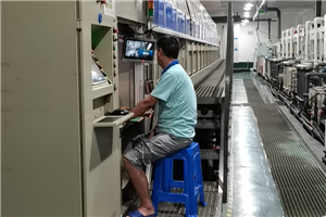
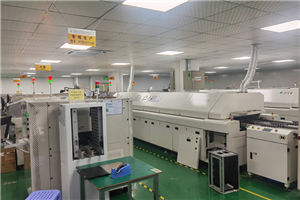
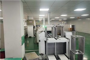
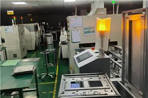
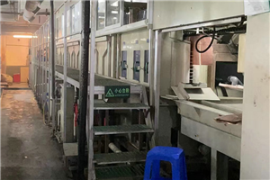
If pursuing cost-effective FPC manufacturing services, choosing a Chinese manufacturer is the best choice. As a manufacturing powerhouse, China has abundant resources, cheap labor, and a large number of technical personnel. We recommend Haibo, a Chinese FPC assembly service provider with over 10 years of experience, who has performed outstandingly in various aspects
Efficient and reasonable quotation:There is an efficient quotation process to assist you in making decisions, providing reasonable prices and highly competitive quotes in China.
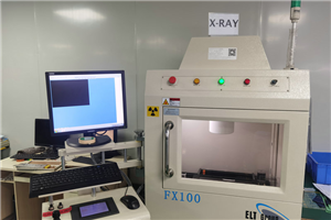
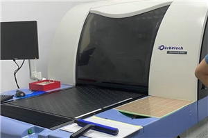
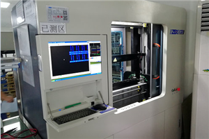
High quality and reliable products:Produce high standard printed circuit boards, manufacture and test according to specifications, international standards, and internal controls, and conduct pre production inspections to ensure robust processes.
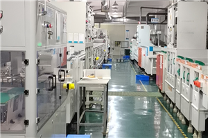
Quick and on-time delivery:The assembly equipment is in good condition, with high productivity, minimal downtime, short delivery time, and also provides urgent services.
Timely and effective response:Always respond to customer needs, provide accurate information, answer questions through multiple channels, and offer one-stop services.
Strong technical strength:China's FPC manufacturing technology is leading, and Haibo has a complete SMT solution that covers assembly, inspection, and other capabilities. It also provides prototype production and customization services.
mobile phone: 86-15113315665
Contact: Chen Changhai
mobile phone: 86-18676922028
E-mall: haibo_fpcba1668@163.com
Address: 3rd Floor, Building 2, Fuxing Industrial Park, Building B, Chuangye 1st Road, Jiangbian Community, Songgang Street, Bao'an District, Shenzhen