1-100 layers of rigid, flexible, and rigid flex PCB
Impedance control, back drilling, backplate, embedded, IC substrate, heavy copper 40 ounces
FR4、 Polyimide, high-speed, high-frequency, metal core, ceramic PTFE、 alumina
Blind holes, buried holes, staggered holes, stacked holes
Blockage of conductive and non-conductive vias
i N i HDI PCB、 Any layer HDI VIPPO
PCB制造是印刷电路板制造的简称,它是将具有电路图案的设计实现为物理和功能的PCB裸板的完整制造过程。
PCB可分为单层线路板,双层PCB,多层板,刚性PCB,柔性印刷电路板和刚柔结合PCB通常。不同类型的PCB具有不同的制造工艺和技术,但一般而言,PCB制造包括以下工艺:基材切割、钻孔、电镀、铜迹蚀刻、阻焊印刷、丝网印刷、表面处理、电子测试、PCB元件放置、功能测试和目视检查。
刚性、柔性、刚柔结合、半柔性、HDI、射频和微波、IC 基板
FR4、聚酰亚胺、Kapton、PET、铝基、铜基、金属基、氧化铝陶瓷、陶瓷、混合材料、无卤素、高速、高频、PTFE、特氟龙
盲孔、埋孔、VIPPO、导电孔塞、非导电孔塞、背钻、阻抗控制、厚铜、金手指、嵌入式
1-40层用于大规模生产,最多100层用于原型制作
PCB厚度:0.10-10.0mm
最大 PCB 尺寸:1500x508mm
HASL、OSP、ENIG、ENEPIG、浸银、浸锡、金连接器、选择性混合饰面。
凭借我们在 PCB 制造领域16年以上的经验,我们已经建立了强大的工程、生产和采购团队,这有助于我们确保能够以最低的价格和高质量供应印刷电路板。
我们所有的 PCB 均按照内部标准生产和检查,例如 IPC-A-600、IPC-A-610 和 UL (E358677) 标准。生产设施严格遵循 ISO9001 和 ISO13485,以确保我们生产的 PCB 具有最高质量。
我们从 2007 年开始供应印刷电路板。我们的工程和生产团队非常了解各种 PCB。我们了解 PCB 的各个方面,包括基材、DFM、生产、测试、检查、故障分析等。
许多客户信任我们超过10年。这是因为我们始终提供优质产品。我们敬业的客户服务团队始终按时回复客户,无论是询价和订单,还是投诉和延迟交货日期。
我们提供各种 PCB,包括标准刚性 PCB、柔性 PCB、刚挠结合 PCB、HDI PCB、高速PCB,高频PCB,铁氟龙印刷电路板,集成电路电路板,嵌入式PCB…此外,我们还可以提供 PCB 制造和 PCB 组装的一站式服务。因此您可以信赖我们来满足您的 PCB 需求。
我们的 PCB 制造标准交付周期为1-4周,具体取决于层数、材料、技术和数量。但我们也可以在24小时内提供快速交付的 PCB。如有任何 PCB 需求,请联系我们。
PCB板的分类很难定义。但最常见的是按层数和所用基材分类。
(1)层数:单面PCB、双面PCB和多层PCB;
(2)所用基板:刚性PCB、柔性PCB、刚柔性PCB。
单面PCB 是成本最低、最简单的 PCB 类型,单面采用一层铜制成。电气元件也只安装在单面上。成本低廉的原因是 PCB 制造服务简单且元件较少。
双面印刷电路板是一种具有两层铜层的电路板,分别为顶层铜层和底层铜层,顶层铜层与底层铜层之间通过通孔连接。
顾名思义,多层PCB 由多个工作层组成,顶层用作放置元件的表面,底层用于布线和焊接。中间的各层具有多种功能,如信号、导体和接地。多层 PCB 由通孔组成,通孔是连接各层走线的垂直结构。制造多层 PCB 始于准备 FR-4 覆铜板和预浸料板。
硬质PCB 是由刚性材料制成的印刷电路板,例如 FR4、金属芯、陶瓷、氧化铝等。刚性 PCB 不能弯曲,但它们为电子元件的组装提供良好的支撑。刚性 PCB 几乎在每个工业领域都有广泛使用,是最常用的电路板。
柔性印刷电路板有利于小型化设备。这种类型的 PCB 广泛应用于各个领域,包括相机、手机和 RFID 卡。表面贴装技术也可用于制造这种类型的 PCB。在回流焊接过程中,需要特殊类型的夹具来固定柔性 PCB。柔性 PCB 具有不同的材料特性,如密度、比热容和热导率。
刚挠结合板将刚性和柔性材料结合在一起,兼具刚性PCB和柔性PCB的优点。由于刚性部件上可以布置高密度的钻孔和导线,因此元件通常都安装在刚性部件上;柔性部件通常用于连接刚性部件,它们可以弯曲或扭曲成不同的形状。
柔性部件通常采用聚酰亚胺材料制成,该材料具有优异的柔韧性、耐热性和加工性能。
因此,刚挠电路板通常用于高科技电子产品,例如智能手机、笔记本电脑、数码相机、机器人等。
印刷电路板广泛应用于工业、医疗、汽车、电信、机器人、能源和电力、测试和测量以及航空航天等各个领域。以下仅列出 PCB 制造商关注的几个常见领域:
这是最常用的娱乐和信息应用类型。典型的例子包括手机、笔记本电脑、电视等。随着电子设备中引入越来越多的功能,印刷电路板制造也适应了多样化的需求。
随着新技术的发展,自动化设备被广泛应用于农业、工业控制系统、机器人、物联网等许多工业领域。这类PCB通常由4层以上的多层电路板组成,有些可能需要高层或 高密度电路板.
几乎所有电子产品都需要电源PCB,用于供电和实现功能。随着新能源,特别是电动汽车和UPS电源的发展,该行业对PCB的需求越来越多。这种PCB通常需要TG 170或以上的高材料,可能需要厚铜,通常从2盎司到10盎司。
可靠性和质量在这类应用中至关重要,因为它与人们的生活直接相关。印刷电路板通常用于制造汽车摄像头以及安全气囊发射器的压力和运动传感器。汽车行业的高要求促使 PCB 制造商进行严格的控制和严格的可靠性测试,以符合汽车标准。
由于医疗设备需要极其谨慎和精确,因此使用 PCB 来控制这些特定功能。一些医疗设备包括起搏器、血压监测器、植入物和手持式监测器。遵守医疗应用的监管要求也很重要。
In this section, we will discuss various materials and layers that help us manufacture PCB boards.
The material sandwiched between copper layers is called a dielectric material. This material can be further divided into core and prepreg. As mentioned earlier, the most commonly used dielectric material is FR4, which is resin impregnated glass fiber. Most PCB manufacturers use FR-4 as the default substrate material.
The solder mask layer is mainly used to protect the copper layer from corrosion caused by exposure to the external environment. The solder mask layer can also guide the solder to move along the copper pad.
The wire core consists of two copper foils and an insulation layer in the middle. Copper is used for conductivity, while insulation layers are used for mechanical support and electrical insulation.
In PCB board manufacturing, prepreg is often mentioned. For multi-layer PCBs, multiple core boards can be connected together. This is a specific use of prepreg, but unlike core boards, prepreg is softer and more flexible. It is made of uncured resin and glass woven fabric. PCB manufacturers place pre impregnated materials between the core board layers and place them under specified temperature and pressure, and the pre impregnated materials will bond the core boards together. After this curing process, the core board and prepreg are almost indistinguishable.
Use layout tools to draw copper wires and pads on each layer, but PCB manufacturers actually start from the complete copper layer. Unnecessary copper in the design is etched away. Copper pads used for surface mount still require surface treatment because copper is now easily oxidized.
As mentioned in the previous sections, the layers are insulated from each other, so a structure is needed to connect the layers. This can be achieved by drilling a copper plated hole to connect the layers. There are also various types of through holes, depending on the design and complexity of the equipment:
Through hole:The most popular and inexpensive method is to connect one layer to another through a through-hole.
Blind:The through-hole connects the top or bottom to the inner layer, but does not pass through all layers.
Buried:This through-hole does not extend to the top or bottom layer as it only connects to the internal layer.
Microchannel:Very small through holes drilled by laser are mainly used for small spacing and high-density equipment.
Due to the need for additional steps such as drilling and copper plating, the manufacturing cost of PCB is highly dependent on the number of vias.
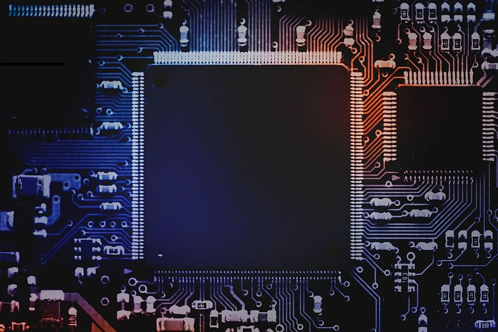
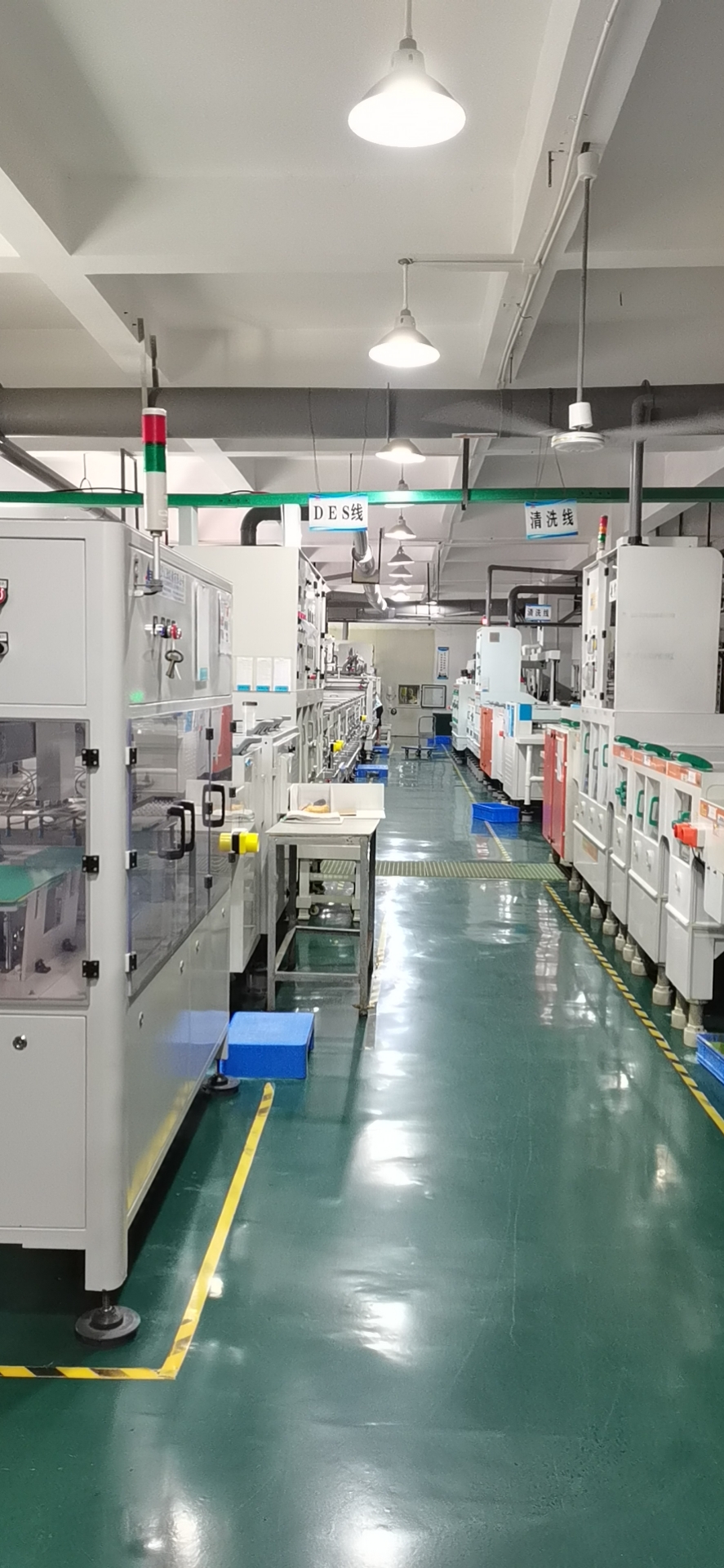
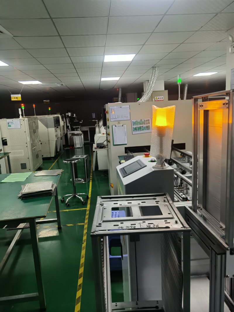
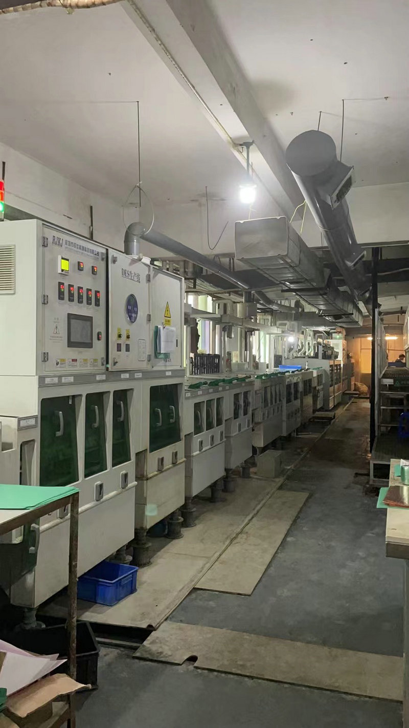
PCB board manufacturing consists of multiple steps, which may vary depending on design, number of layers, component layout, and complexity. The following are the main processes involved in PCB manufacturing:
In order to design a fully functional circuit, it is necessary to first use computer-aided design (CAD) software systems to generate circuit designs. The design workflow begins with circuit development, layout definition, and CAD program generation. Allocate circuit components to different CAD layers based on expected functionality. In addition, the layout provides detailed instructions on component placement, routing, and component packaging types. The goal is to include as much data as possible for reference. From CAD tools, generator tools are used to develop control programs for manufacturing PCBs.
The use of the industry recognized light painting tool "Gerber" is the foundation for manufacturing PCBs in printed circuit board manufacturing equipment. A complete set of Gerber files must be sent to the PCB manufacturer, including the complete generated files for each layer.
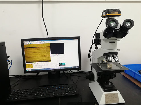
The patterning process can be completed through photolithography. In photolithography, a photosensitive material (also known as photoresist) is coated on a copper foil and then exposed to light. During the exposure process, a photomask is used to cover the patterns required for the manufacturing of printed circuit boards. Apply the solution to the exposed part of the PCB to dissolve the photosensitive material. Use another solution to etch away soluble photosensitive materials and unwanted copper foil. Then leave a pattern similar to the photomask on the copper foil. Finally, remove the residue through a cleaning solution. The basic process of PCB board manufacturing can be summarized as: exposure, development, etching, and peeling.
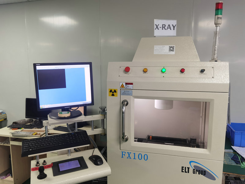
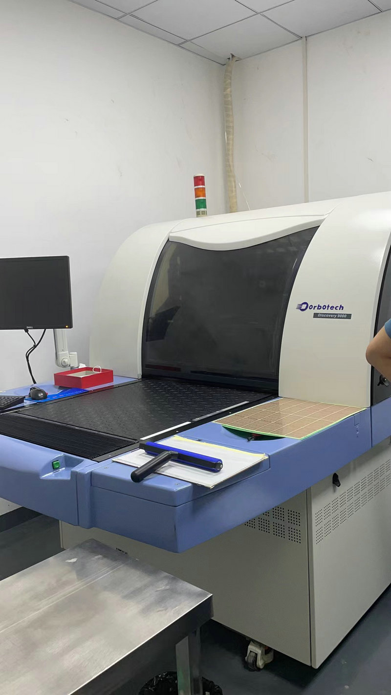
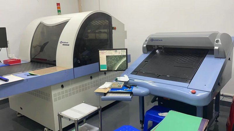
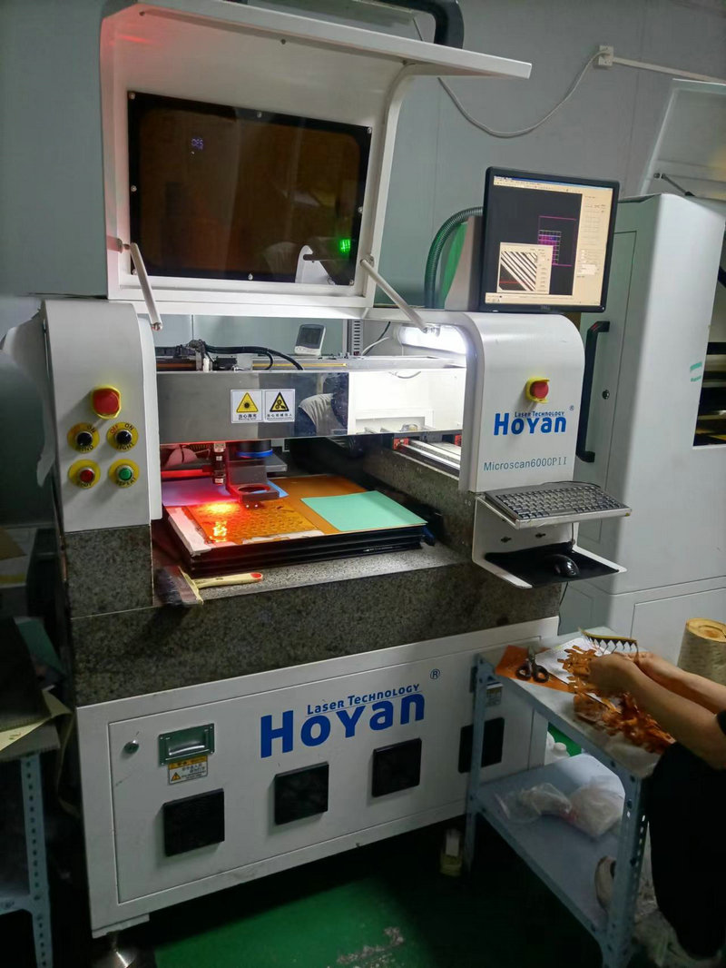
Recall that through holes are structures that connect different layers. This is achieved through the use of mechanical or laser drilling. The drilling process is often a bottleneck in PCB manufacturing services. The quality of drilling can be evaluated by the burr height, diameter, and roundness of the hole. These quality issues are mainly affected by the wear and degradation of drilling tools.
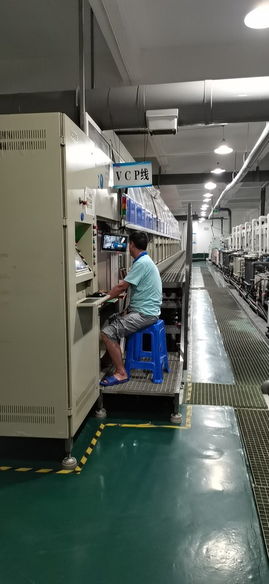
The inner wall of the through-hole should be plated with copper, which is a conductive material that can electrically connect different layers of the vertical structure. PCB manufacturers can choose between electrolytic or chemical plating methods. During the electroplating process, copper ions react in the chemical plating tank, and this chemical reaction is called the "reduction" process. Then transfer the copper plated material from the seed layer (or source) to the surface of the through-hole. During the electroplating process, the copper source is ionized by incorporating an electric field into the system.
As mentioned earlier, the solder mask layer is a thin protective polymer layer deposited on the FR-4 laminate, which helps to isolate conductive and insulating surfaces. The solder mask layer can be achieved through various direct and indirect deposition techniques. The application of solder mask varies depending on the classification and type of solder mask to be used. Thermosetting solder mask layer (also known as epoxy liquid) is screen printed onto the substrate and then thermally cured. Due to its faster curing time, UV solder mask layers are also widely popular. Due to its high precision and resolution, photosensitive solder mask is the most common type in the PCB manufacturing industry. The ideal solder mask should have strong adhesion, low refractive index, low coefficient of thermal expansion (CTE), and high thermal stability.
Through HASL OSP、ENIG、ENEPIG、 Surface treatments such as immersion in gold, silver, and tin protect exposed copper wires on PCB copper pads from external environmental influences. Here, we will discuss the most commonly used ones: HAP, OSP, and ENIG.
Hot air solder leveling (HASL): After using cured solder resist to manufacture PCBs, place the circuit board into a hot molten solder bath to form intermetallic compounds. According to the Restriction of Hazardous Substances Directive (RoHS), alternative surface treatment methods such as HASL are being adopted.
Organic Solderability Protective Agent (OSP): This is another commonly used surface treatment method, which is based on organic molecules forming a surface treatment film.
Chemical nickel gold plating (ENIG): The process flow of ENIG includes surface acid washing, etching, activator treatment, chemical nickel plating, and immersion gold plating. ENIG is definitely the most popular surface treatment method for manufacturing PCBs.
Screen printing is used to indicate some circuit board information, such as component placement, wiring, and other functions, which are useful during PCB manufacturing services. Templates containing specific patterns are installed on top of printed circuit boards. The opening on the template indicates the information to be transferred to the PCB, and then use a scraper. After removing the template, the pattern with information remains on the circuit board and is then baked to solidify the material.
The main steps of manufacturing multi-layer printed circuit boards are the same as the above process, except that some additional steps need to be performed to achieve the final stacking. In order to achieve multi-layer PCB, multiple pre impregnated materials (glass fiber materials) need to be stacked on a copper-clad laminate. The copper-clad laminate in PCB manufacturing is a product of the lamination process. This process involves applying copper foil to both sides of FR-4 substrates or "laminates" bonded together by heat and pressure. Heating will trigger a chemical reaction in the bonding layer, thereby bonding the PCB layers together.
Drill holes after final lamination. Pattern on a single layer. Since the component does not come into contact with the inner layer, surface treatment is not required. Then perform other conventional processes on the multi-layer board, such as through-hole filling, pattern application, and electroplating.
We can divide PCB manufacturing defects into appearance defects and functional defects. Both of these defects are important for ensuring 100% PCB quality.
Appearance defects are defects that affect the appearance of PCB, such as pinholes, excessive etching, insufficient etching, and damage. Such defects will not directly affect the functionality of the circuit board, but may pose a threat to humans after prolonged use.
Functional defects refer to serious defects that have adverse effects on the operation of PCBs. This type of defect includes short circuits, conductor fractures, or open circuits.
These PCB board manufacturing defects may be caused by contamination, high parameters, plating issues, or incorrect etching processes. PCB can withstand pressure caused by vibration, temperature changes, and other harsh environmental stresses. Therefore, testing is required after PCB board manufacturing.
In order to meet quality assurance, large-scale PCB manufacturing services adopt automatic optical inspection (AOI), online testing (ICT), flying pin testing, and X-ray testing. These commercial tests are used to locate manufacturing defects in printed circuit boards through reliable inspection and testing techniques (using electrical or non electrical, non-contact methods).
Automatic optical inspection uses image processing software to inspect PCBs through reference comparison method. This software has a defect detection algorithm that can be compared with defect free PCBs. This helps PCB manufacturers detect defects and avoid potential hazards. This is usually accomplished by conducting pixel by pixel analysis and comparison to identify changes and locate defects.
Online testing is the best testing method for mass production of PCB boards. This testing method uses fixtures (also known as nail beds) to test the circuitry of PCBs. This type of PCB performance verification method is in automatic mode, involving capacitance and resistance testing. ICT has efficient testing throughput and high diagnostic accuracy, which can provide fast feedback for short circuits and open circuits.
Flying needle testing is the most suitable testing method for small-scale production and prototype design, as it is slower than ICT. This type of testing uses movable probes to contact PCB test points and circuit pads. The movement of the probe is controlled through programming; Therefore, due to its ability to access any contact point on the circuit board, this test has the advantage of testing high-density and complex circuits. Flying needle testing does not require customized fixtures, making it highly cost-effective for small businesses.
The future of printed circuit boards is full of promising innovations and the latest technologies to provide better functionality and efficiency. In recent years, research and industry have been studying 3D electronic products, which allow for direct printing of conductive traces on device surfaces. This technology can achieve higher functionality and more complex designs, while allowing for space saving and weight reduction.
The Internet of Things (IoT) and artificial intelligence are also the main driving forces behind PCB manufacturing technology. The progress in these fields has made breakthroughs in the large-scale production of electronic devices, allowing for the storage of more data while miniaturizing the devices. Miniaturization has driven further design improvements and manufacturing of flexible PCBs and HDI circuits.
When PCB manufacturers attempt to manufacture PCB boards, the rise of automotive applications such as ADAS (Advanced Driver Assistance Systems) and electric vehicles will continue to impact the PCB market. ADAS requires better vehicle sensing systems, such as lane assist systems and passenger detection systems, which increases the demand for in car electronic devices.
When PCB manufacturers prepare to manufacture PCBs, sustainability is also taken into consideration. As environmental issues become increasingly important, recycling technology is also constantly being researched. Government policies will also play a key role in the growth of the printed circuit board manufacturing market by subsidizing expenditures, providing incentives, encouraging investment, and focusing on research and development.
If pursuing cost-effective FPC manufacturing services, choosing a Chinese manufacturer is the best choice. As a manufacturing powerhouse, China has abundant resources, cheap labor, and a large number of technical personnel. We recommend Haibo, a Chinese FPC assembly service provider with over 10 years of experience, who has performed outstandingly in various aspects
Efficient and reasonable quotation:There is an efficient quotation process to assist you in making decisions, providing reasonable prices and highly competitive quotes in China.
High quality and reliable products:Produce high standard printed circuit boards, manufacture and test according to specifications, international standards, and internal controls, and conduct pre production inspections to ensure robust processes.
Quick and on-time delivery:The assembly equipment is in good condition, with high productivity, minimal downtime, short delivery time, and also provides urgent services.
Timely and effective response:Always respond to customer needs, provide accurate information, answer questions through multiple channels, and offer one-stop services.
Strong technical strength:China's FPC manufacturing technology is leading, and Haibo has a complete SMT solution that covers assembly, inspection, and other capabilities. It also provides prototype production and customization services.
mobile phone: 86-15113315665
Contact: Chen Changhai
mobile phone: 86-18676922028
E-mall: haibo_fpcba1668@163.com
Address: 3rd Floor, Building 2, Fuxing Industrial Park, Building B, Chuangye 1st Road, Jiangbian Community, Songgang Street, Bao'an District, Shenzhen