Laser cutting and electropolishing templates (EPStencil)
Surface mount technology (SMT), through-hole technology (PTH), and hybrid technology
Assembly of rigid, flexible PCB and rigid flex combination PCB
Small to medium batch production
Passed ISO9001:2015 ISO 13485: 2016 certification and UL certification
100% electronic testing, AOI, X-RAY, ICT, and FCT
有两种已知的方法将电子元件连接或安装到印刷电路板上---通孔技术(THT)和表面贴装技术(SMT)。THT 是一种 PCB 组装方法,其中元件引线通过将其插入电路板的钻孔中来连接到 PCB。另一方面,SMT 利用焊膏技术将无源和有源元件安装到 PCB 中。
SMT 是目前广泛使用的最新技术,有时与 THT 结合使用。在 SMT 中,在焊料印刷过程中使用 PCB 模板,以便能够有效地将焊料分配到电路板的接触垫中。有关 PCB 模板的更多详细信息将在以下部分中讨论。
PCB 模板是表面贴装技术 (SMT) 中的重要工具,能够将正确数量的焊膏沉积到印刷电路板的准确位置。它是一种厚而扁平的金属,由相当于电路板上的焊盘的孔组成。模板包含基准标记,可在加工过程中用作对准参考。模板印刷是实现快速焊料沉积以供大规模生产使用的最实用方法。
电路板模板印刷工艺是SMT的第一步,常用于单面PCB组装和双面 PCB组装一个成功的SMT工艺应该对以下几个关键变量进行优化研究,如模板厚度和孔径、焊膏状态和金属填料尺寸、刮刀速度、压力和角度等。这里我们讨论了在PCB模板中使用焊膏印刷工艺。
首先,我们需要将 PCB 放在焊膏印刷机上。PCB 组装用的模板将被固定并夹紧,以避免移动。自动和手动印刷机均可使用。
当 PCB 模板准备好后,就该在电路板模板中添加适量的焊膏了。但请确保焊膏事先混合均匀,因为焊膏需要储存在4°C至10°C的环境中。
将 PCB 板夹紧并与电路板模板对齐,使得孔与要沉积焊料的接触垫重合。
然后刮刀在电路板模板上移动,将焊膏均匀地分布到 PCB 模板孔中。焊膏将穿过孔并最终粘附到 PCB 焊盘上。
将电路板模板与电路板分离,然后松开电路板并移至下一工序。对于细间距焊盘,建议以直线运动方式进行分离,以制作精确印刷的焊膏。
进行焊锡印刷后光学检查,以验证焊锡膏的量和排列是否正确。内置俯视摄像头用于自动检查沉积的焊锡膏。焊锡膏检查过程可以由焊锡膏印刷机(如果该机器具有此功能)完成,也可以由单独的检查机完成。
确保焊料印刷质量一致性的强制性步骤是清洁模板。清洁对于去除粘附在孔壁上的焊膏残留物非常重要。必须定期进行清洁,以避免焊膏沉积物硬化并影响下一步工序。对于更精细的组件,清洁更为关键。模板清洁可以手动或自动完成。现代电路板模板印刷机具有喷雾槽,可用于在印刷后清洁 PCB 中的模板。
以下是设计 PCB 组装制造模板的不同考虑因素和技术。
在单面和双面 PCB 组装中,电路 PCB 模板有各种形状和尺寸。最常见的形状是圆形和矩形孔。也可以设计其他孔形状以支持要安装的元件的形状。必须考虑焊膏类型、焊盘尺寸和元件间距,设计具有合适的长度、宽度和厚度。厚度会影响焊膏的体积。细间距 PCB 可能需要更薄的模板以减少焊料溢出和桥接。过厚可能会导致焊膏因表面张力而粘附在孔壁上。
与 Gerber 设计相比,一些电路板模板孔径被有意设计成具有较小的孔径面积,以便在回流过程中焊膏塌陷时扩散。IPC 标准描述了 PCB 模板设计中的两个重要尺寸参数——面积比和纵横比。面积比是 PCB 焊盘面积与孔壁面积之比,而纵横比则考虑了孔径宽度和模板厚度。电路板模板的尺寸还受焊球尺寸或焊膏的金属填料尺寸的影响。
在实际的PCB组装中,特别是双面印刷电路板组装,PCB 中最常见的模板类型是由不锈钢制成的,因为它具有耐腐蚀性、耐用性和尺寸精度。不锈钢在重复使用时不易变形,最适合大批量 PCB 组装。有时使用聚合物 PCB 模板,它们是由 Kapton 制成的柔性材料。它们不太优越,不太适合大批量 PCB 组装。
对于更复杂的 PCB,还可以设计多阶模板或阶梯式模板。这些类型的电路 PCB 模板在单个孔径中具有不同的厚度。这通常适用于细间距组件,其中需要在模板设计 PCB 的开口中创建局部减小的面积。多层模板通常通过初始化学蚀刻工艺和随后的激光蚀刻来制造。
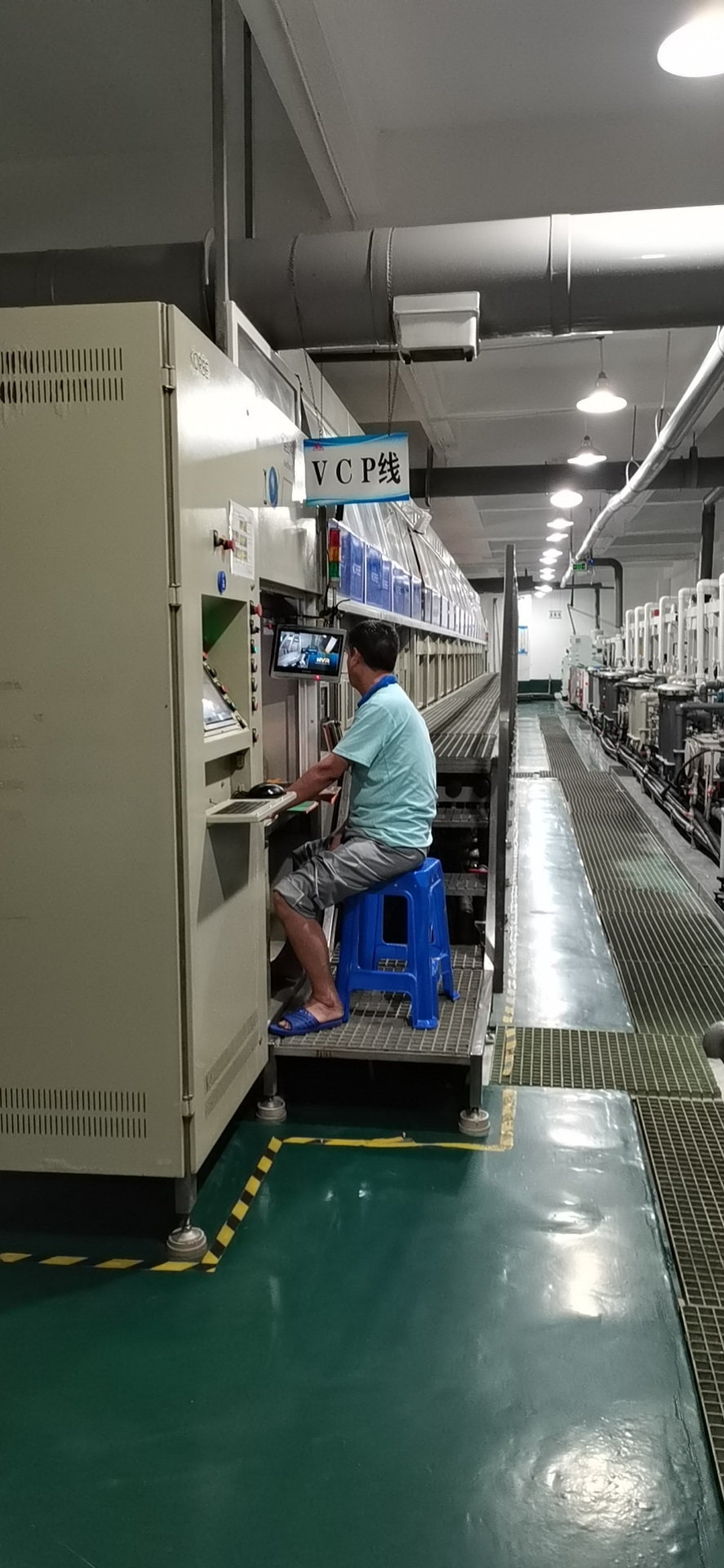
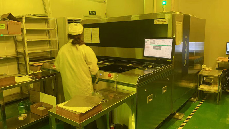
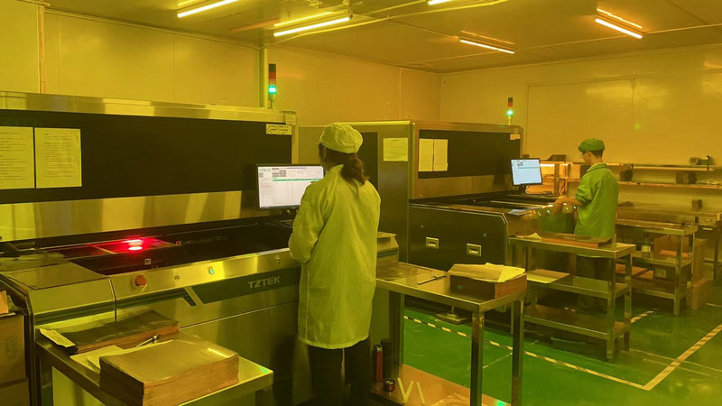
The template used for PCB assembly manufacturing is made by referencing the PCB design layout with Gerber file data. Each template manufacturing technique produces different hole wall qualities. The quality depends on the roughness and accuracy of the template holes. The following are different template manufacturing technologies adopted by the industry.
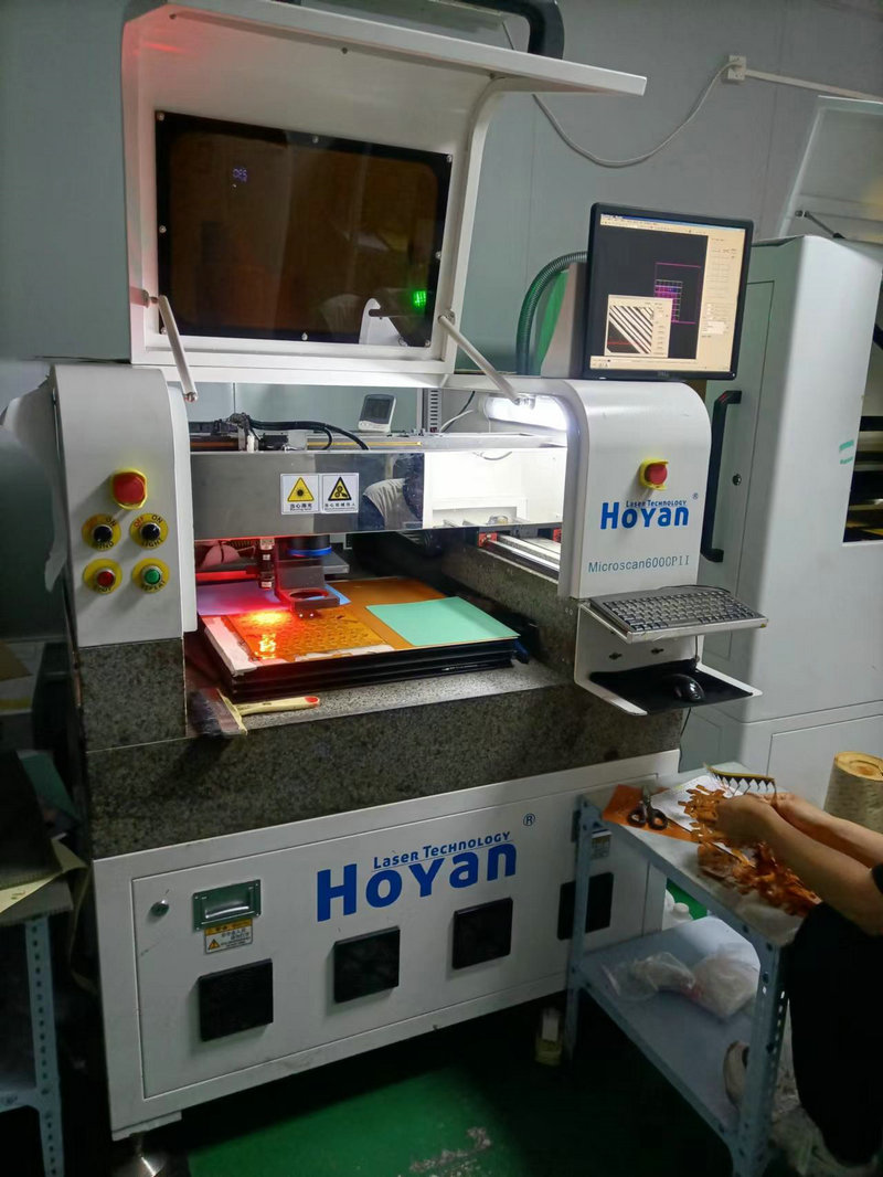
Laser cutting is most suitable for forming precise apertures with neat edges. It is most suitable for fine spacing and high-density design. Laser cutting can produce trapezoidal aperture, making it easier to release solder paste. Therefore, laser cutting PCB templates are widely used.
Chemical etching uses subtraction to form patterns on templates. Firstly, clean the metal surface and cover it with photoresist. Then use chemicals to develop and rinse the photoresist. Etch unwanted metal with etchant spray.
Unlike other techniques, electroplating is an additive method that uses nickel. Electroforming is sometimes combined with laser cutting to obtain more precise PCB template apertures.
The following lists possible issues that may arise from poor design of circuit board templates, as well as solutions proposed based on our experience.
Inaccurate alignment between the circuit board and PCB template may result in printing misalignment.
The template is 100% accurate and the alignment should also be completed correctly.
Incorrect aperture geometry may cause solder overflow and bridging during printing and reflow processes.
Ensure the aperture is correct and inspect the template with PCB before printing solder paste.
The template opening is too narrow, which can lead to insufficient solder volume and incomplete solder coverage.
Experienced engineers will develop appropriate template files. After completion, compare the template with the PCB pads.
In addition to reflow soldering issues, the side of PCB templates may also be affected by template thickness and aperture size.
Adopt appropriate template thickness and aperture, and use solder ball templates.
If pursuing cost-effective FPC manufacturing services, choosing a Chinese manufacturer is the best choice. As a manufacturing powerhouse, China has abundant resources, cheap labor, and a large number of technical personnel. We recommend Haibo, a Chinese FPC assembly service provider with over 10 years of experience, who has performed outstandingly in various aspects
Efficient and reasonable quotation:There is an efficient quotation process to assist you in making decisions, providing reasonable prices and highly competitive quotes in China.
High quality and reliable products:Produce high standard printed circuit boards, manufacture and test according to specifications, international standards, and internal controls, and conduct pre production inspections to ensure robust processes.
Quick and on-time delivery:The assembly equipment is in good condition, with high productivity, minimal downtime, short delivery time, and also provides urgent services.
Timely and effective response:Always respond to customer needs, provide accurate information, answer questions through multiple channels, and offer one-stop services.
Strong technical strength:China's FPC manufacturing technology is leading, and Haibo has a complete SMT solution that covers assembly, inspection, and other capabilities. It also provides prototype production and customization services.
mobile phone: 86-15113315665
Contact: Chen Changhai
mobile phone: 86-18676922028
E-mall: haibo_fpcba1668@163.com
Address: 3rd Floor, Building 2, Fuxing Industrial Park, Building B, Chuangye 1st Road, Jiangbian Community, Songgang Street, Bao'an District, Shenzhen