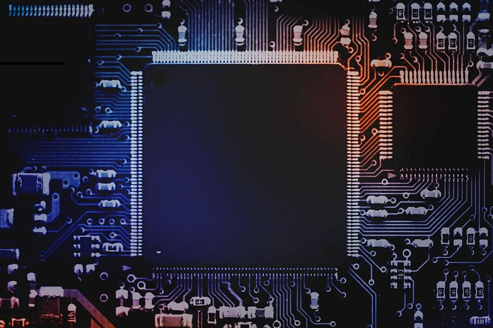
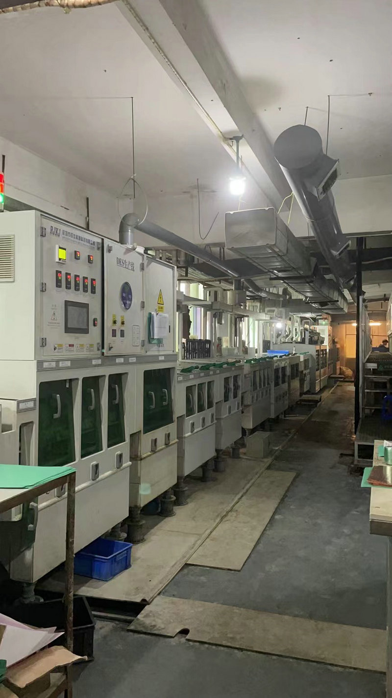
With the development of technology, electronic products are becoming increasingly miniaturized, and the size of PCBs is also getting smaller. In this situation, the aperture of micro holes used for connection and positioning in PCBs is gradually decreasing, which poses certain challenges for drilling micro hole PCBs.
The reason why laser drilling technology can be widely applied in many fields is because its technology has high peak power and fast processing speed. However, in PCB production, the quality of micro porous PCB processing will have a significant impact on the quality of the PCB. Therefore, using laser drilling technology for micro hole PCB processing during PCB production will result in higher quality PCBs. And it provides convenience for the assembly and use of PCBs. Therefore, it is necessary to strengthen the application research of laser micro hole PCB processing technology in the production of printed circuit boards, in order to better promote the development of the PCB production industry.
Overview of laser drills used in micro porous PCBs
In the design and production of micro hole PCBs, laser micro hole processing technology uses laser drilling technology to process micro holes with a diameter less than 50um, which is a mature micro hole processing technology. At present, laser micro hole processing technology can be used for processing various materials in micro hole PCBs, and the size of micro holes is directly related to the energy density, type, wavelength, and PCB board thickness of the laser. Due to the different absorption coefficients of different materials for laser wavelengths, we also need to use lasers of specific wavelengths to process specific PCB materials.
In principle, laser micro hole processing technology for micro porous PCBs mainly uses two methods: photothermal ablation and chemical ablation to process micro porous PCBs. Photothermal ablation enables materials to absorb high-energy lasers in a very short period of time, heating them to a molten and evaporated state, thereby achieving the goal of processing micro porous PCBs. This technology can form holes in PCBs under high energy, but the hole walls will leave blackened carbide residues, so the material needs to be cleaned before perforation.
The use of chemical ablation etching technology is actually the use of lasers with wavelengths less than 400nm to break down the long molecular chains of organic materials, turning them into tiny particles. When the energy of the molecules is greater than that of the original molecules, they will detach from the material, and under strong external force adsorption, the material will be quickly removed, thus becoming micropores. Using this technology, there will be no carbonization phenomenon on the surface of the material, and only a simple cleaning of the hole wall is required.
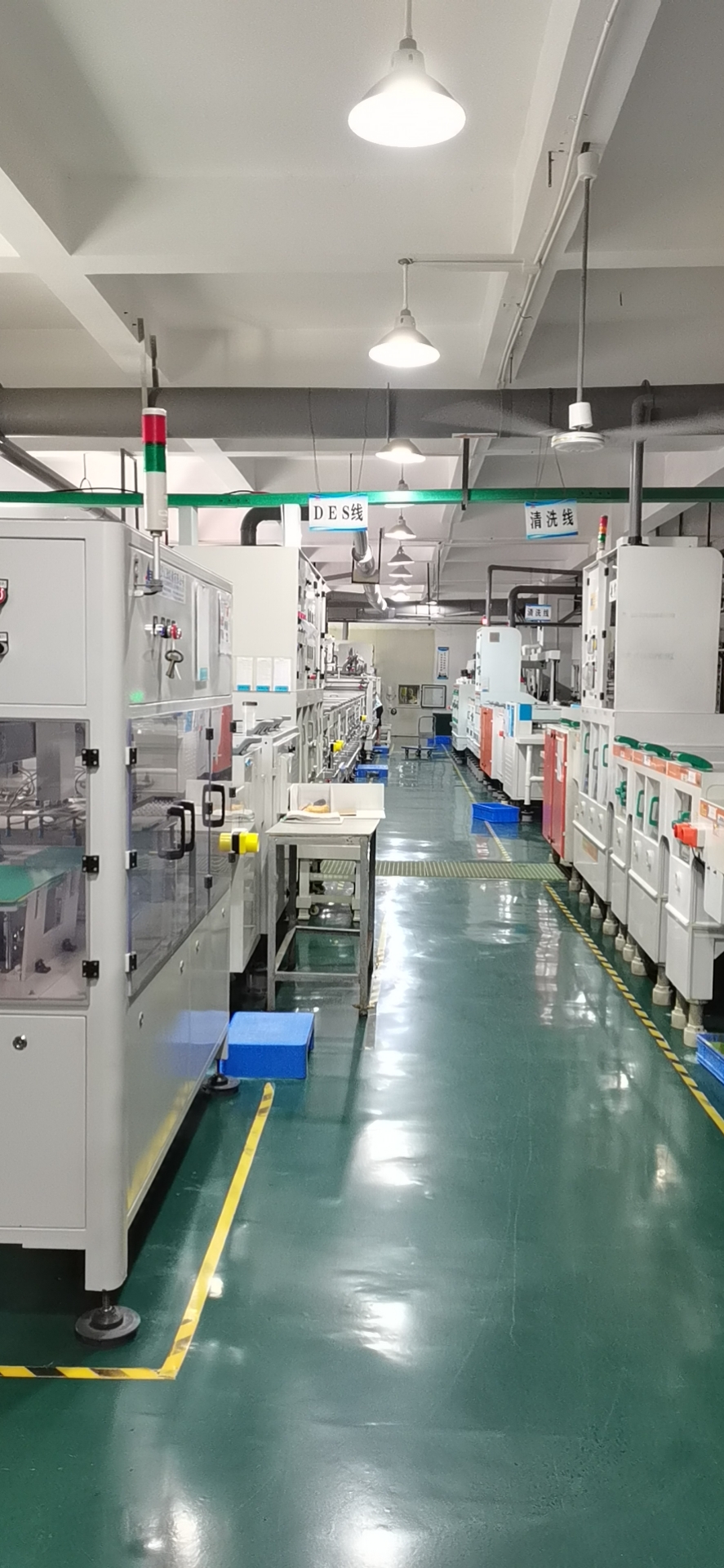
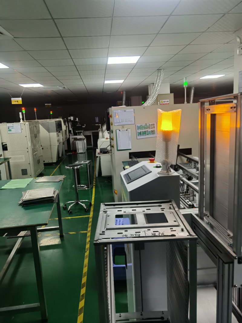
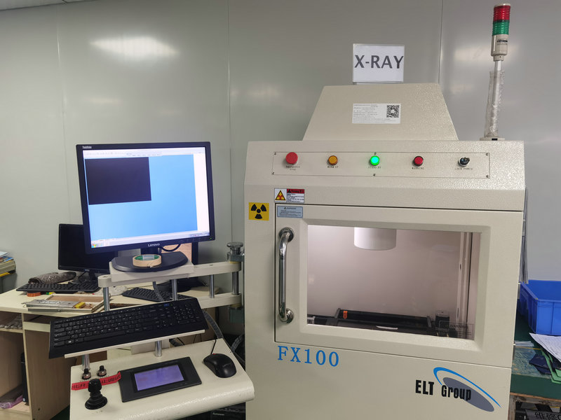
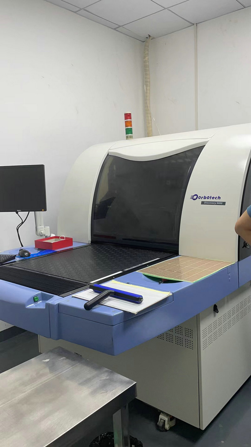
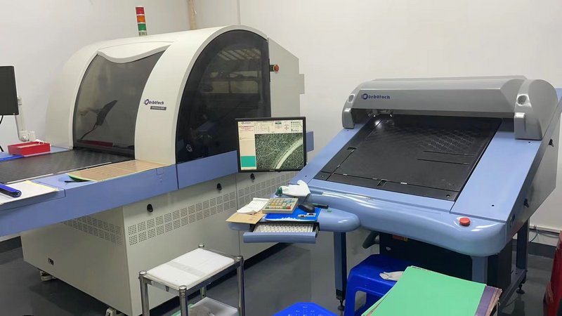
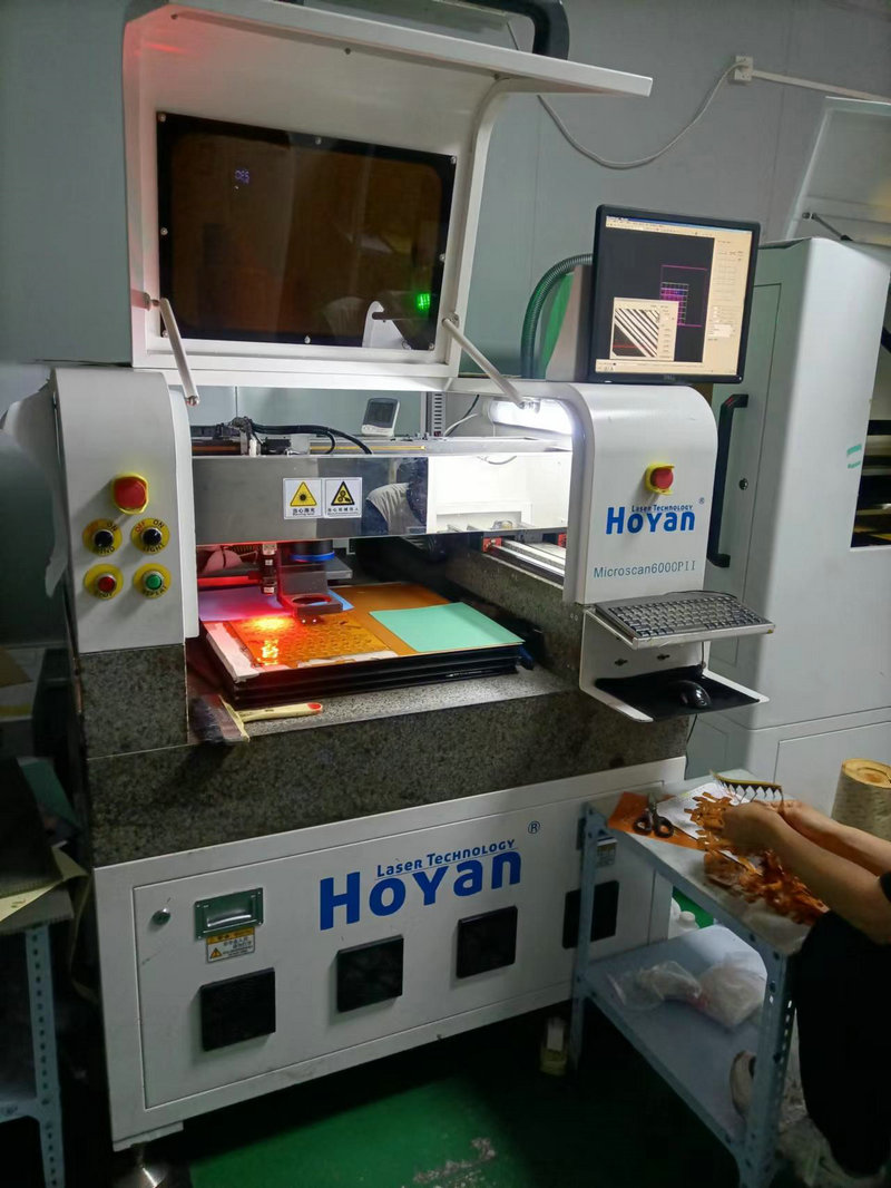
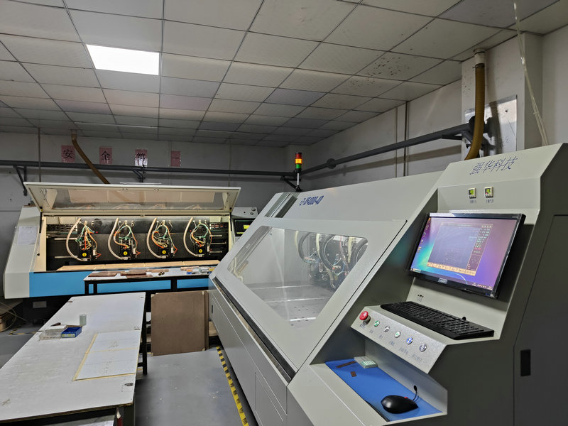
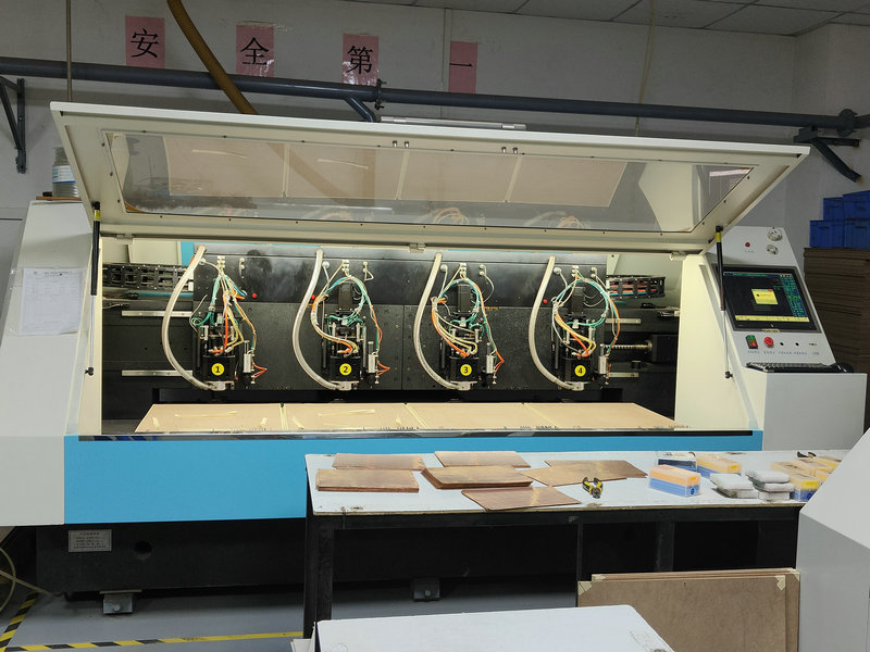
Equipment required for laser drilling in the production of microporous PCBs
There are currently three main types of laser micro hole processing equipment used in PCB production: molecular lasers, carbon dioxide lasers, and ultraviolet Nd: YAG lasers.
Molecular laser
Using a molecular laser, PCB can be processed with a 248nm short wave ultraviolet laser, which has good absorption of this light. At the same time, the laser pulse generated by the device can reach a peak power of several megawatts as long as it lasts for 20ns. After homogenization, the beam can generate a flat topped waveform, which is then projected onto the formed mask plate, corroding the bottom of the PCB material. Using this device can result in clean and smooth holes, but due to the slow corrosion rate, hundreds of laser pulses are required.
CO2 laser
Using a carbon dioxide laser, infrared waves with a wavelength of 10.6 μ m can be output. Compared with ultraviolet solid-state lasers, using this laser can achieve greater processing depth. In specific applications, it is necessary to select the center of the beam according to the metal aperture stop, focus the beam on a lens with a focal length of 4 inches, and then irradiate the surface of the circuit board.
Ultraviolet Nd: YAG laser
Using a UV Nd: YAG laser, it can output laser light at 260-1060nm. Compared with molecular lasers, this laser pulse energy is lower, but the peak power obtained is the same. Due to the Gaussian distribution of the laser beam obtained by using this device, more small light spots can be obtained. Therefore, this device can complete small-sized micro hole processing.
By comparison, using molecular laser processing can achieve higher laser resolution and complete the processing of clean holes. At present, this technology is mainly applied to the processing of Polyimide materials, which can use larger beam masks to simultaneously process holes. By using carbon dioxide laser processing, materials containing FR4 can be processed to obtain micro pores with smooth pore walls and uniform pore cone. But the disadvantage of using this device is that the quality of the holes obtained is not very good, and standard cleaning processes need to be used to clean the completed holes. By using YAG laser, smooth and straight hole walls can be obtained, and holes smaller than 50um can also be processed. At present, this type of equipment is mainly used for the processing of aluminum oxide PCB materials.
Three laser drilling techniques in microporous PC
In the production of micro porous PCBs, UV solid-state lasers can better dissolve copper materials, couple better with polymers such as glass, and obtain smaller spot sizes, thus achieving better applications. However, in actual production, when using laser processing technology for micro hole processing, three processing techniques can be used to produce micro hole PCBs, namely laser punching, laser sleeve hole, and laser spiral processing.
Laser drilling technology
In micro porous PCBs, laser drilling technology requires keeping the laser beam stationary when needed, and then using high repetition rate pulses to process the material. Therefore, the size of the hole is determined by the size of the light spot. This technology can be used to process small diameter through holes.
Laser sleeve hole technology
Laser drilling technology is to make the focused laser spot walk around the through-hole once, and with each rotation, the depth of the hole will deepen by one circle. Using this technology requires calculating the processing depth for each rotation, but if this technology is used, undissolved material will be left in the middle of the hole, so it cannot be used for blind hole PCB processing.
Laser spiral machining
Laser spiral machining can be used to process large-sized through holes. Specifically, the focused laser beam is moved outward from the center of the hole in a spiral shape to corrode the PCB material layer by layer. Based on the size of the through hole, material characteristics, and layer parameters, parameters such as screw pitch and number of runs are determined. Through numerical control programming, micro hole PCB processing can be completed.
summarize
After analysis, laser micro hole PCB processing technology can be well applied in the PCB production process. However, in actual production, it is still necessary to choose suitable processing techniques based on different process equipment and process characteristics in order to better complete the processing of different PCB materials.