Materials: High TG FR4, Halogen free FR4, High speed FR4, PI (Polyimide) PET、 Aluminum, copper, alumina ceramics, special alloys, microwave and radio frequency, PTFE FR4 mixture, ceramic FR4 mixture
Layers: The prototype has 1-100 layers
Control impedance as low as 5%
Copper thickness (oz): 1/3 oz to 20 oz
Blind hole, buried hole, inner hole of welding plate, stacked hole, staggered hole
Technology: Backboard, Backdrill, countersunk hole
随着电子行业的技术飞速发展,许多公司都希望在很短的时间内生产出电子产品。为了满足电子市场的这一需求,PCB 制造商开发了一种称为“快速周转”的制造服务,可以缩短周转时间 PCB制造 从几周缩短到几天,甚至24小时。
随着对快速周转印刷电路板的需求不断增长和严格要求,制造商想出了一种快速生产 PCB 的方法,成本低,性能高。这种快速制造称为快速周转 PCB 制造,可通过高生产速度和卓越的制造技术实现。快速周转 PCB 制造为各种应用提供了某些优势,例如可扩展性、灵活性和可定制性。
快速周转 PCB 板是可以在比标准 PCB 更短的时间内制造并交付给客户的电路板。它们通常用于快速周转 PCB 原型制作,使工程师能够快速测试和改进其设计而不会出现重大延迟。
快转PCB在我国发展迅速。 海博是中国一家值得信赖的快速周转印刷电路板制造商,专门从事原型和中小批量快速 PCB制造. 我们的快速周转 PCB 交货时间为:
原型:1-3 天(甚至 24 小时)
小型系列:1周
为什么快速 PCB 制造对于您的企业来说是一个可行的选择?以下是您从快速制造印刷电路板中可以获得的一些好处:
提交后立即 PCB设计,一家快速生产制造公司将对电路板的可制造性进行评估。审查将包括识别制造过程中可能导致延误的潜在风险。如果目标是缩短产品验证时间,则快速生产 PCB 制造最适合用于构建原型。大多数快速生产 PCB 制造公司都会在其网站上公布加急选项的交货时间。
在快速周转 PCB 制造中,产品可以更早地投放市场。由于周转时间较短,尤其是原型设计,设计中的错误很容易被发现。可以尽早发现制造问题,从而减少大批量生产期间昂贵的修复费用。快速周转制造也是一个非常好的营销手段,因为这意味着客户和用户的便利性和更少的麻烦。因此,快速周转 PCB 制造商可帮助品牌所有者节省总体成本。
快速印刷电路板制造可应用于原型设计、预生产和批量生产。这意味着供应商可以提供从小批量到大批量的此类制造。可制造性设计或 DFM 是设计和原型设计阶段的一项重要要求,它使工程师能够评估材料、原理图和布局是否经过优化以实现易于制造、组装和检查。
在快速 PCB 制造中,设计可以在短时间内得到评估,从而为迭代和测试留出更多空间。这让项目所有者能够灵活地相应地调整设计、重新运行和重新测试,并快速验证设计。新技术和复杂功能的出现给制造商带来了挑战,但快速制造提供了灵活性和适应性,使其在市场上保持领先地位。中国快速 PCB 制造商非常擅长提供灵活的一站式服务。
Fast turnover PCB manufacturers typically state in their technical manuals and websites which types of printed circuit boards can be produced quickly. Some manufacturers only focus on standard FR-4 PCBs, but some manufacturers can also produce all types of PCBs, such as soft or hard flex or rigid boards, including high-density interconnect (HDI), depending on the available machines and tool types. Rapid manufacturing has a wide range of applicability, depending on the capabilities and service types of rapid manufacturing PCB manufacturers. The following are the various stages of products that can be applied for rapid manufacturing.
Rapid production of PCBs is an effective method for identifying and reducing design risks, especially in situations where product development time sensitivity is high. Due to the fact that the prototype is only produced in small batches, rapid production is a wise choice as it can obtain results in advance and provide sufficient space for further evaluation and improvement.
During the transition to production operation, a slightly higher quantity than the prototype batch will be run to simulate the performance of the printed circuit board. Some issues cannot be captured in small samples, so larger and more reasonable statistical sample sizes will be generated to understand whether the final design is indeed manufacturable. At this point, another batch of rapidly converted PCB boards may be needed for pre production testing.
Fast delivery of PCBs is also suitable for production operations, where early delivery is crucial. If the initial stages such as prototype design and pre production run are successfully passed, mass production will be smoother.
Let's be pragmatic, risks exist at every stage. There is no perfect design and production, especially in the initial stage. Being able to predict which factors will affect turnover time will help you understand the options to take. This will help to obtain the best fast turnover PCB without any errors.
The process capability of PCB manufacturers is crucial in the rapid production of PCBs. Manufacturers with rich experience and excellent rapid production capabilities can quickly produce PCBs. PCB manufacturers need to equip themselves with appropriate types of equipment and personnel to quickly complete all work from engineering to manufacturing and testing.
If the fast turnover PCB manufacturing company provides outdated and slow equipment, the compressed schedule will be difficult to meet. Each machine has different capabilities and units per hour (UPH). High speed machines that can meet customized PCB design have higher advantages in fast turnover manufacturing. Some suppliers, especially experienced companies, can provide flexibility in machine backup and simultaneous operation. For example, a company with multiple drilling machines will offer higher production capacity and provide alternative solutions in case of machine failure. Some Chinese fast turnover PCB manufacturers are using the most advanced equipment.
The procurement time of materials will significantly affect the delivery time of fast PCB manufacturing. We have inventory of the most commonly used materials, but some special materials may take several weeks to purchase.
Design engineers will check the availability of materials before designing PCB for rapid turnover. The selected materials play a crucial role in quickly completing the product. Suppliers must ensure material availability, as production cannot begin if materials are restricted. A good procurement strategy is to plan alternative materials and suppliers to cope with unavoidable shortages.
Undoubtedly, printed circuit boards with complex through-hole structures will have longer delivery times due to additional and complex drilling processes. More stacking or layers also mean longer lamination cycles, thereby affecting the overall project schedule. In short, PCB design can greatly affect the manufacturing and assembly time of printed circuit boards. Therefore, fast turnover PCB companies should work closely with designers to optimize PCB design.
The manufacturing complexity of circuit boards is also important. For example, higher-level HDI boards require longer delivery times, while simple double-layer PCBs can be produced quickly. With the development of equipment and technology, fast turnover PCB manufacturers are able to supply increasingly complex types of circuit boards.
Engineering configuration is usually necessary throughout the entire manufacturing process, especially during setup and inspection. This is one of the reasons why engineering expertise is extremely important. If a fast turnover PCB company does not have sufficient resources and good engineering judgment, some decisions in the manufacturing process may not be provided in a timely manner, which may affect the PCB fast turnover schedule.
Special process requirements can also affect the delivery cycle of fast PCB boards. For example, countersunk holes, peelable masks, hard gold coatings, VIPPO through-hole plugs, etc.
Quality control and planning may also affect the production time for rapid PCB production. IPC Level 3 standard PCBs require longer time for quality inspection.
For fast turnover PCB services, every day is important. You may be concerned that Chinese fast turnover PCB suppliers may not be able to meet your requirements. But it is very easy to transport goods from China to other countries in the world. Air freight usually takes one week, while sea freight takes 3-4 weeks. But the delivery may take 2-3 working days.
To obtain a finished product, a fast printed circuit board needs to go through the following steps.
Firstly, computer-aided design (CAD) must be used to develop PCB designs. Design is the blueprint for the subsequent process. The design phase is the stage of defining the circuit layout and schematic. Different circuit components are filled into each PCB layer.
All relevant details of the PCB must be specified in the design document. The format type submitted to fast PCB manufacturers is called "Gerber file", which is a known board layer format in the industry. The Gerber file indicates what the device should follow and where it should go. The aperture library and drilling files are sent separately, and they determine the hole size to be referenced.
The output of any PCB design is preliminary, which lists the substrates, copper foils, and other materials required to build a printed circuit board. The PCB file format is usually Gerber 274 format, which is widely accepted by PCB manufacturers. In the Gerber file, PCB materials are clearly written, such as FR-4, aluminum, ceramic, etc PTFE、 Polyimide, etc.
The patterning process is the use of photolithography and other techniques to transfer designs onto copper plates. Photolithography technology utilizes photoresist, which is a photosensitive material that can dissolve or not dissolve under light. This process can print the required copper patterns onto the board.
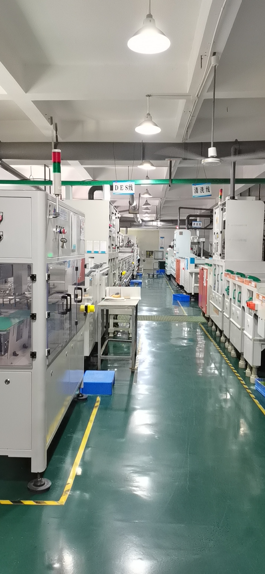
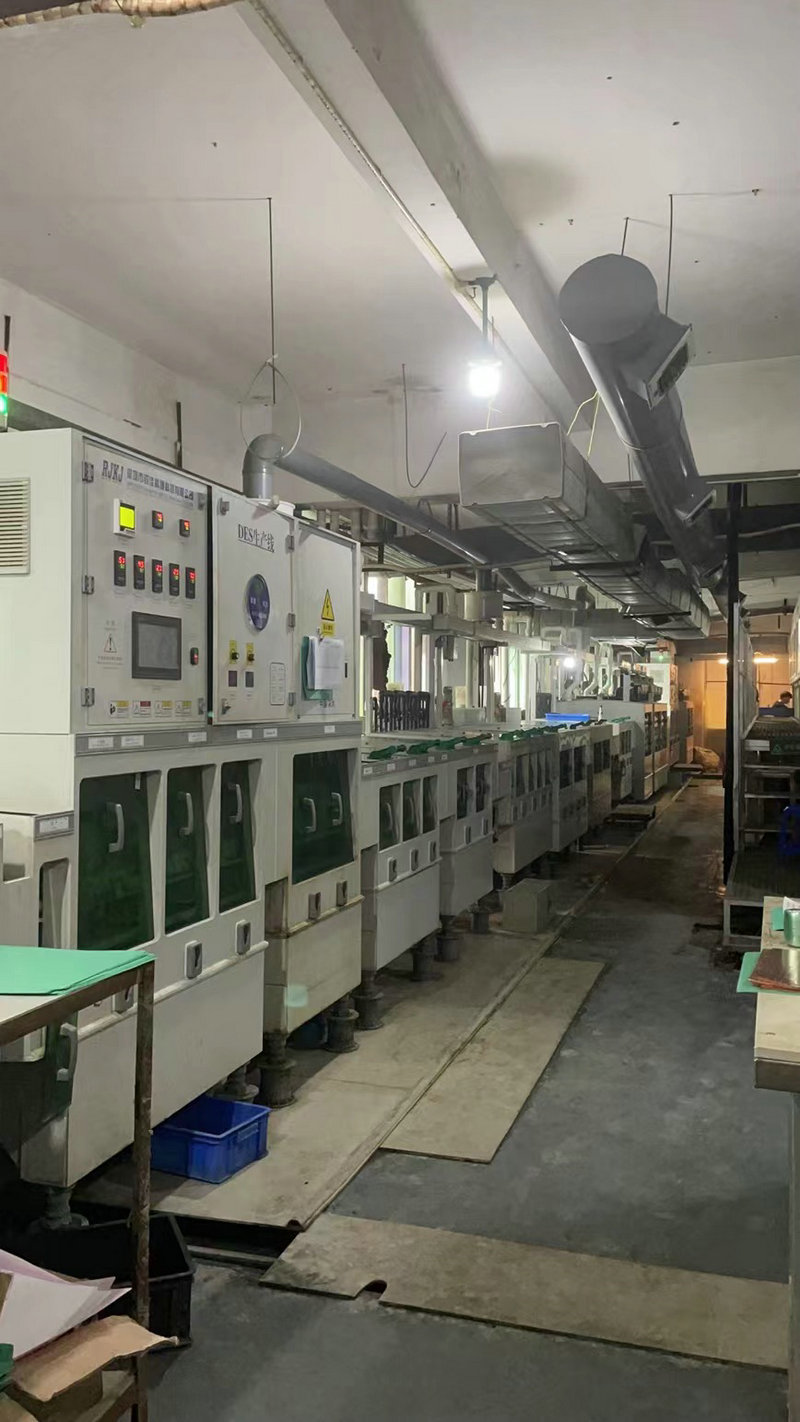
The circuit board with patterns undergoes etching process to remove unwanted copper foil, leaving the expected traces and patterns on the PCB. After the corrosion etching process, use a stripping solution for cleaning.
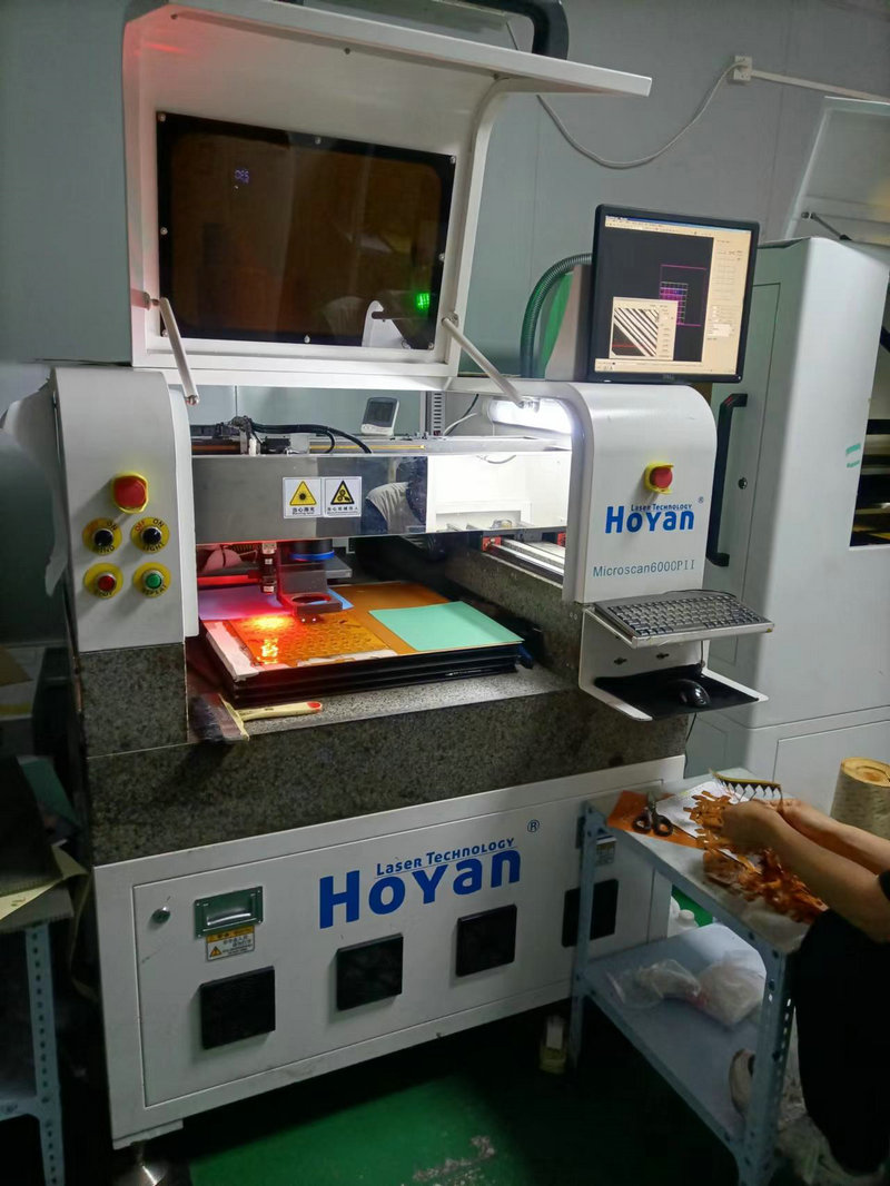
Next, specialized equipment will be used to drill holes in each layer, which can be accomplished through mechanical or laser methods. PCBs with higher density and smaller holes usually require longer processing time, resulting in higher costs.
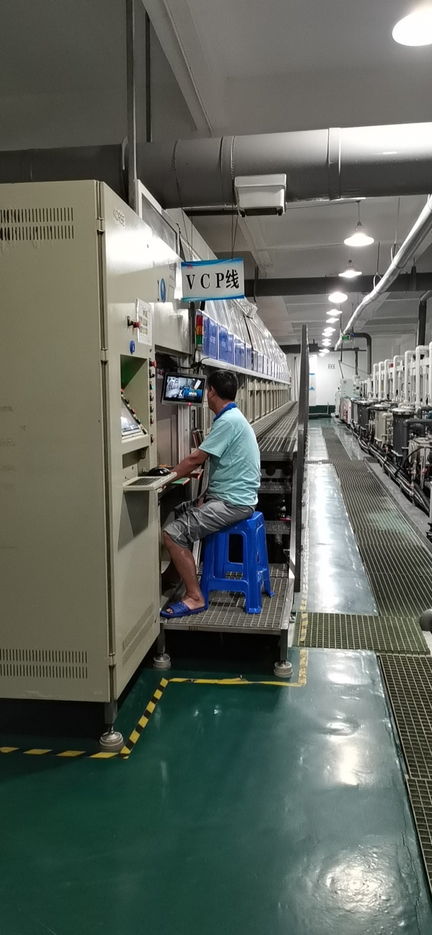
Due to the fact that holes or vias serve as connections between layers, they are plated with copper to form conductive paths between the layers of the PCB. Copper plating also has another function, which is to increase the copper thickness of the copper wire.
The solder mask layer is printed on the top and bottom of the PCB to protect the copper area outside the solder pads.
Screen printing, also known as component marking, is a component marking printed on the surface of a PCB to clarify the position of components, which is very useful for the installation, repair, and maintenance of components. PCB assembly process
The exposed copper pads on the PCB can also be surface treated with various chemicals to protect them from changes in environmental temperature and humidity. Due to the easy oxidation of copper, surface treatment or finishing is an extremely important step. The most commonly used PCB surface treatments are HAL, ENIG, and OSP.
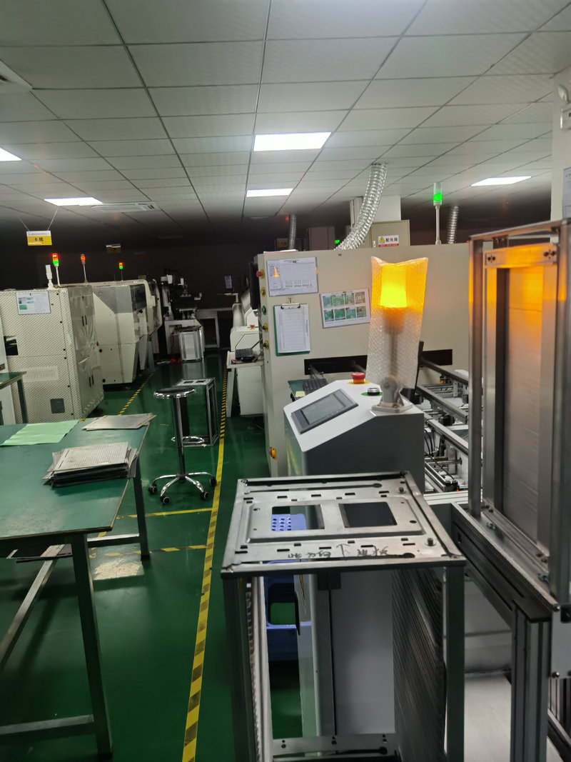
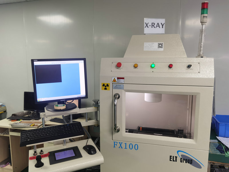
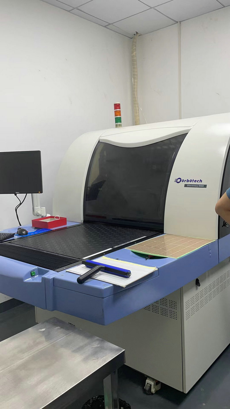
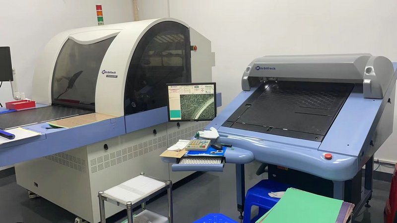
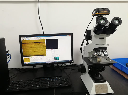
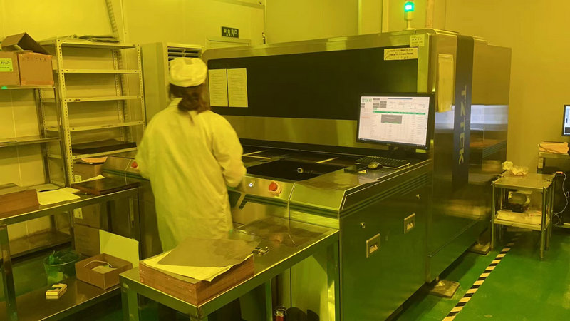
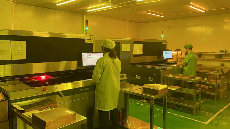
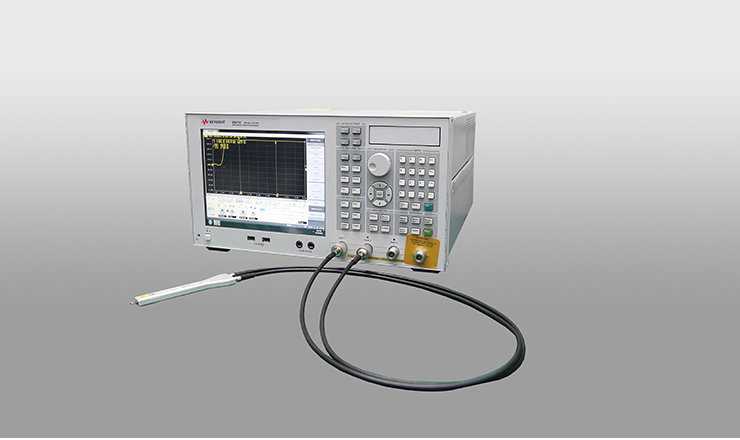
The main purpose is to manufacture circuit boards that meet design and functional requirements; Therefore, PCBs should undergo visual inspection processes such as automatic optical inspection. For fast PCB manufacturing, these are still necessary steps to understand defects and issues as early as possible.
The PCB still needs to undergo testing to check for circuit issues such as short circuits and open circuits. For small-scale manufacturing and prototype design, a flying pin tester can be used to access the contact pads. For large-scale production, online testing is a better choice because the operation time is faster.
Now that you have learned some basic knowledge of fast PCB manufacturing, we will discuss the different factors to consider when choosing a suitable fast supplier.
Time is the golden requirement for achieving rapid turnover of PCB projects. A suitable supplier should have shorter delivery times and develop detailed strategies to follow the promised schedule. In order to meet the urgency of construction, every process should be efficient, as any delays and non-standard work in the process will slow down the entire project. Potential delays should have corresponding mitigation plans in place to address the issue immediately. Most rapid turnover manufacturing supplier websites list typical turnover times to guide customers in making decisions.
Suppliers should have advanced machines with sufficient functionality and capability to support fast PCB type processing. Manual work only interferes with the process because it is slow, prone to errors, and prone to error handling. With decades of development in PCB manufacturing, China's rapid PCB manufacturing technology is at the forefront of the world.
Suitable suppliers should also be able to provide lower costs. Like any business, this is a factor that determines the success or failure of a transaction. Ensure understanding of the scope, terms, and conditions specified in the submitted quotation to prevent communication barriers and further modifications. Suitable suppliers will also provide advice on how to maintain flexibility in payment and how to reduce costs. Chinese fast turnover PCB manufacturers can produce high-quality circuit boards in a short period of time.
With suitable suppliers, quality should also exist in every process and every field. This means that fast turnover PCB manufacturing companies follow a quality management system, which includes a series of rules and standards that need to be followed. Due to the high technological content of printed circuit boards, various certification bodies such as UL (Underwriters Laboratories) and IPC have outlined requirements and guidelines for designing and manufacturing high-quality, safe, and reliable electronic products.
Good customer service is also crucial to ensure the smooth progress of design, pre production, and mass production. Some rapid manufacturing suppliers only respond at the beginning of the project, but this is not the case. Throughout the entire lifecycle of the product, suitable suppliers should still be involved and committed to responding quickly and promptly to technical and non-technical inquiries.
If pursuing cost-effective FPC manufacturing services, choosing a Chinese manufacturer is the best choice. As a manufacturing powerhouse, China has abundant resources, cheap labor, and a large number of technical personnel. We recommend Haibo, a Chinese FPC assembly service provider with over 10 years of experience, who has performed outstandingly in various aspects
Efficient and reasonable quotation:There is an efficient quotation process to assist you in making decisions, providing reasonable prices and highly competitive quotes in China.
High quality and reliable products:Produce high standard printed circuit boards, manufacture and test according to specifications, international standards, and internal controls, and conduct pre production inspections to ensure robust processes.
Quick and on-time delivery:The assembly equipment is in good condition, with high productivity, minimal downtime, short delivery time, and also provides urgent services.
Timely and effective response:Always respond to customer needs, provide accurate information, answer questions through multiple channels, and offer one-stop services.
Strong technical strength:China's FPC manufacturing technology is leading, and Haibo has a complete SMT solution that covers assembly, inspection, and other capabilities. It also provides prototype production and customization services.
mobile phone: 86-15113315665
Contact: Chen Changhai
mobile phone: 86-18676922028
E-mall: haibo_fpcba1668@163.com
Address: 3rd Floor, Building 2, Fuxing Industrial Park, Building B, Chuangye 1st Road, Jiangbian Community, Songgang Street, Bao'an District, Shenzhen