为了确保最高质量 印刷电路板 为了向客户提供优质产品,我们会在 PCB 生产过程中或 PCB 完成后进行大量测试和检查。以下是我们进行的主要测试和检查。
IQC (Incoming Quality Control) is a key process to ensure the quality of PCB (Printed Circuit Board). This is a complete inspection system designed to detect any defects or inconsistencies in any materials we use in PCB manufacturing. These materials include the most important CCL, copper, dry film, solder mask, screen printing, and so on.
IQC should pay great attention to details, as defective PCBs may cause significant losses to us and our customers. IQC can not only save costs through defect detection, but also help maintain a high level of customer satisfaction by ensuring that products are manufactured to the highest standards. Therefore, IQC is crucial for producing reliable and high-quality PCBs and should be taken seriously.
Although we use AOI (Automatic Optical Inspection), electrical testing, and other testing/inspection methods in the PCB manufacturing process, many areas still require manual visual inspection. For example, visual defects in the substrate, solder mask layers, defects in screen printing, etc., because these small defects cannot be detected by equipment. Manual visual inspection involves a detailed visual inspection of the PCB to detect any visual defects or flaws before sending the circuit board out for use.
This inspection confirms to us and our customers that the product will comply with IPC-A-600 Level 2 or Level 3 standards and customer standards. We ensure that our inspection process complies with the latest industry standards and best practices. Therefore, our inspectors have sufficient training and experience, and can use the required testing equipment.
Nowadays, although advanced AVI (Automatic Visual Inspection) machines have been developed, we believe that manual visual inspection is still needed.
AOI uses high-resolution cameras to capture PCB images from different angles, and then compares them with reference images to detect any defects or inconsistencies. Therefore, manufacturers can quickly identify problems in the production line without slowing down production time or affecting quality control.
By utilizing AOI in the PCB manufacturing process, manufacturers can detect errors before they become costly issues. It helps reduce waste and improve overall efficiency, as it can quickly identify and discard PCBs that can pass inspection without AOI. Manufacturers can use AOI technology on PCB production lines to meet strict quality standards while ensuring consistency of the final product.
In our PCB process, we mainly use AOI to inspect subtle defects in copper wires, such as copper wire voids. In addition, AOI is also used in solder mask processes to detect solder mask issues.
Therefore, we believe that Automatic Optical Inspection (AOI) is an important component of PCB manufacturing to ensure that PCBs are defect free and meet the highest quality standards.
FAI is an essential tool for PCB manufacturers as it ensures that their products can operate as expected. It also allows them to detect problems early in manufacturing, thereby avoiding costly rework or production line scrapping.
In the PCB production process, any problem at any stage may result in the entire batch being scrapped. Therefore, we need to first ensure that the PCB meets 100% customer and industry standards. Therefore, before mass production, we will run several prototypes as the first piece and check if the first piece meets all standards.
By conducting FAI, PCB manufacturers can also ensure that their PCBs comply with industry standards, such as the IPC-A-600 acceptance criteria. In addition, it can ensure that all PCBs produced by PCB manufacturers have the highest quality and meet customer requirements.
Microsection inspection involves taking a small sample from each PCB and examining it under a microscope to identify any defects or inconsistencies. By doing so, manufacturers can identify potential issues during the production process or after installation to prevent them from becoming costly problems.
We believe that the most critical element in PCB is copper plating. If there is no appropriate copper plating thickness and conditions, the PCB will not function properly or be durable. At Haibo, we will conduct 4 micro slicing and inspections during the PCB manufacturing process to check whether the copper plating thickness is sufficient and whether there are any defects in the copper plating. In addition to checking the copper plating, we will also check whether the dielectric thickness is the same as the design and whether the solder mask thickness meets the IPC-A-600 acceptance criteria.
Microsection inspection is an essential step in PCB manufacturing, as it can help us detect any hidden defects and ensure the quality of the finished product. In addition, it also helps to identify potential issues during or after the production process, avoiding them becoming costly problems.
We all know that PCB (printed circuit board) is an important component of many electronic devices, and the performance and reliability of PCB largely depend on its electrical integrity. Therefore, in the PCB production process, open/short circuit electrical testing is essential to ensure that all PCBs meet the required specifications before delivery to customers.
Open/short circuit electrical testing can detect any defects or inconsistencies in PCB wiring, which may lead to subsequent performance issues or safety hazards. Therefore, electrical testing is crucial for PCB production and must be executed accurately to ensure the production of high-quality PCBs that meet all requirements.
Electrical testing requires the use of specialized testing machines or fixtures. Firstly, the PCB must be connected to the testing machine, and then voltage must be applied and the current monitored for any abnormalities. Then the test results should be recorded, as this information is very useful for future PCB inspections.
At Haibo, we use two electrical tests to detect open/short circuits. The first type is suitable for prototype flying needle testing, and the second type is nail bed testing. These two testing methods each have their own advantages and disadvantages, as shown below:
attribute | Flying needle test | Nail bed testing |
---|---|---|
Cost of testing equipment | tall | M Medium |
Fixed device required | not have | Yes |
test speed | low | tall |
reliability | tall | tall |
With the improvement of the working speed of digital circuits, the transmission rate of signals on PCB boards is also increasing. For example, the signal rate of PCI Express has reached 2.5Gb/s, the signal rate of SATA has reached 3Gb/s, and the working rate of new standards such as PCI Express II, XAUI, and 10G Ethernet is even higher. With the increase of data rate, the rise time of signals will become faster. When signals with fast rising edges encounter impedance discontinuities on the circuit board, they will produce significant reflections, which will change the waveform of the signal. Therefore, line impedance is a key factor affecting signal integrity.
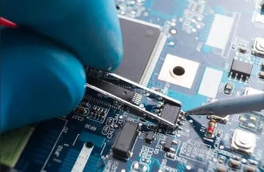
For high-speed circuit boards, ensuring the continuity of impedance on the signal transmission path is crucial to avoid significant signal reflections. Correspondingly, for testing, it is also necessary to test the impedance changes on the signal transmission path of the high-speed circuit board, analyze the cause of the problem, in order to better locate the problem. For example, both PCI Express and SATA standards require measuring the impedance of transmission lines.
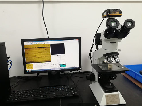
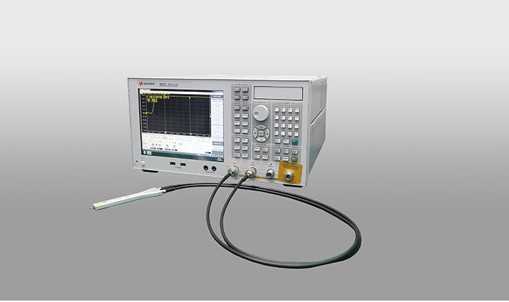
A fast and effective method for impedance testing is the Time Domain Reflectometer (TDR) method. Its working principle is based on transmission line theory, and its working mode is somewhat similar to radar. As shown in the figure below, when a step pulse is added to the tested line, reflection will occur at the impedance discontinuity point. If the source impedance (Z0) is known, the impedance (ZL) of the measured point can be calculated based on the reflection coefficient (ρ).
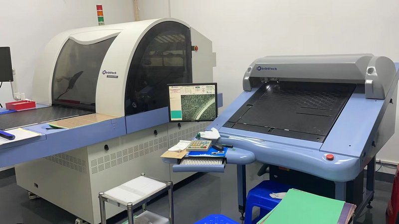
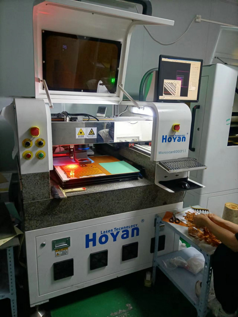
Through TDR impedance testing, PCB manufacturers can ensure that their products meet all impedance requirements without the need for lengthy and repetitive testing processes. It provides fast and accurate impedance measurement, and helps ensure reliable PCB quality and signal transmission. By using TDR impedance testing, PCB manufacturers can save time, money, and resources while ensuring high-quality PCBs for customers.
After the PCB is completed, all necessary tests and inspections have been carried out, and we need to ensure that the PCB components can be easily soldered onto the PCB. Therefore, we will conduct solderability testing by simulating the wave soldering process. Through this process, we can determine whether there are any defects in the welded components. At the same time, we can also identify whether there are issues with solder mask detachment or delamination after the high-temperature PCB assembly process.
Ultimately, PCB solderability testing is crucial to ensure that both SMD and PTH components can be smoothly soldered onto the PCB, whether using a reflow oven for wave soldering SMD assembly or a wave soldering machine for PTH assembly.
If pursuing cost-effective FPC manufacturing services, choosing a Chinese manufacturer is the best choice. As a manufacturing powerhouse, China has abundant resources, cheap labor, and a large number of technical personnel. We recommend Haibo, a Chinese FPC assembly service provider with over 10 years of experience, who has performed outstandingly in various aspects
Efficient and reasonable quotation:There is an efficient quotation process to assist you in making decisions, providing reasonable prices and highly competitive quotes in China.
High quality and reliable products:Produce high standard printed circuit boards, manufacture and test according to specifications, international standards, and internal controls, and conduct pre production inspections to ensure robust processes.
Quick and on-time delivery:The assembly equipment is in good condition, with high productivity, minimal downtime, short delivery time, and also provides urgent services.
Timely and effective response:Always respond to customer needs, provide accurate information, answer questions through multiple channels, and offer one-stop services.
Strong technical strength:China's FPC manufacturing technology is leading, and Haibo has a complete SMT solution that covers assembly, inspection, and other capabilities. It also provides prototype production and customization services.
mobile phone: 86-15113315665
Contact: Chen Changhai
mobile phone: 86-18676922028
E-mall: haibo_fpcba1668@163.com
Address: 3rd Floor, Building 2, Fuxing Industrial Park, Building B, Chuangye 1st Road, Jiangbian Community, Songgang Street, Bao'an District, Shenzhen