1-100 layers of rigid and flexible combination plates, used for prototypes
Blind and buried holes, stacked and staggered holes, arbitrary layer HDI
Micro pores, VIPPO (plated holes inside solder pads)
Blocking through holes using conductive and non-conductive materials
Backdrill, backplate, embedded devices, IC substrate
Passed ISO9001: In 2015 ISO13485: 2016 certification and UL certification
盲孔和埋孔 PCB 是具有盲孔和埋孔的 PCB。镀通孔 (PTH) 是从顶层到底层的通孔。而盲孔是从外层(顶层或底层)到内层的通孔。当通孔的两侧都埋在 PCB 的内层时,它们被称为埋孔。因此,埋孔在 PCB 制造后是看不见的。
我们采取以下措施 6层HDI PCB 举例来说:第1层到第2层有盲孔,第3层到第4层有埋孔,第1层到第6层有镀通孔。所以盲埋孔是高密度PCB中常用的一种,也叫高密度互连PCB。
盲埋孔技术可以节省空间,提高EMC,增强电路中信号的完整性,在高密度和复杂电路设计中具有重要意义。盲埋孔PCB同时具有盲孔和埋孔,这使得这种PCB可以承载更复杂的电路,应用领域也很广泛。
In addition to the reduction in line width, the size of DIP plug-in holes has also been reduced from 1mm to 0.6mm for SMD, and further reduced to below 0.4mm, but it still occupies the surface area of the PCB. Therefore, blind buried holes have emerged in some high-tech PCB manufacturers.
And everyone likes smaller and more exquisite products, so electronic products are constantly being updated and replaced. As electronic products become smaller, lighter, and thinner, printed circuit boards have also developed into soft boards, rigid flex joint boards, blind hole boards, buried hole boards, and so on to meet the needs of electronic products.
Buried hole is a type of through-hole that exists in blind buried hole plates, which is a through-hole between the inner layers. After the lamination process, it cannot be seen in the blind buried hole PCB, and it does not occupy the outer layer area. Both sides of the buried hole are in the inner layer of the circuit board. Taking the 6-layer blind buried hole PCB as an example, the through holes in L2-L3, L2-L4, L2-L5, L3-L4, L3-L5, and L4-L5 are all buried holes, which means they are buried inside the board, so they are called buried holes. This type of PCB is also called buried hole PCB or buried hole PCB.
Buried hole PCBs have a more complex manufacturing process than traditional multi-layer PCBs, so from the perspective of PCB manufacturers, the cost will be higher. Traditional multi-layer PCBs require drilling holes after lamination, while buried hole PCBs require drilling holes in the inner layer before lamination. Drilling needs to be completed in specific inner layers. First, press the specific inner layers together, then drill and electroplate, and finally perform complete pressing to form a complete PCB.
Due to the fact that this operation process requires more time and cost than board through holes and blind holes, it is the most expensive for printed circuit board manufacturers. This process can increase the space utilization of other circuit layers and is typically used for high-precision PCB manufacturing.
Blind holes are from the outer layer to one or more inner layers. One side of the blind hole is on the outer layer, and the other side leads to the inside of the board, but it will not penetrate the entire board. Taking the 6-layer PCB as an example, the vias in L1-L2, L1-L3, L1-L4, L1-L5, L2-L6, L3-L6, L4-L6, and L5-L6 are all blind holes. That's why it's called a blind hole. A PCB with blind holes is called a blind hole PCB or blind hole PCB.
The use of buried holes and blind holes is an excellent method to increase the density of multi-layer PCB manufacturing, reduce the number of circuit board layers and circuit board size. In addition, blind hole and buried hole PCB suppliers have significantly reduced the number of plated through holes. In blind hole and buried hole PCB design, almost all BUM (Building Multi Layer PCB) boards use buried hole and blind hole structures.
Please note that most of the buried holes and blind holes used in blind buried hole plates have small diameters, such as 0.05-0.15 millimeters, so we also refer to this type of PCB with micropores as a microporous PCB. The buried hole is located in the inner layer. The production of buried hole PCBs is the same as that of double-sided PCBs. Blind holes are produced by CNC machines that control the depth of the z-axis and are used to drill small holes, but now with the continuous development of technology, laser drilling, plasma etching holes, and photo induced holes are commonly used.
Blind buried hole laser drilling usually uses three types of machines: carbon dioxide laser machine, excimer laser machine, and YAG ultraviolet laser machine. Here is a brief introduction to Hitachi's carbon dioxide laser machine. The laser wavelength of this machine is 9.4nm, and it can drill one blind hole in three times. It can drill 30000 blind holes on blind buried PCB per minute, with extremely high efficiency.
With the development of electronic products towards high density and precision, customized PCB manufacturers also need to develop corresponding printed circuit boards to match. The most effective way to increase PCB density is to reduce the number of through holes on the board, and accurately set up buried holes and blind holes in blind buried hole PCBs.
Blind holes are located on the top and bottom surfaces of buried blind hole circuit boards, with a certain depth, used for connecting the surface and inner layers. The depth of the hole usually does not exceed a certain proportion. Blind holes are a type of through-hole that connects the inner wiring of a PCB with the surface wiring of a blind buried hole board. Blind holes do not penetrate the entire board.
The buried hole is located in the inner layer of the PCB and does not extend to the surface of the printed circuit board. It is a hole that only connects the wiring between the inner layers, so it cannot be seen from the surface of the blind buried hole board.
The blind buried hole PCB design is located at the top and bottom layers, and has a relative height to connect the outer circuit layer and the inner circuit layer. Usually, the depth of holes in blind buried orifice plates has a specified ratio (the depth cannot be greater than the diameter of the hole). The drilling depth must be appropriate. If it is not suitable, electroplating holes will be difficult. Therefore, few blind buried hole PCB manufacturers choose this printing method. To achieve this blind hole manufacturing process, holes can be drilled in some of the layers that should be connected, and then pressed together. However, this blind hole manufacturing method requires more precise positioning and alignment equipment from the blind hole PCB manufacturer.
There are three different methods for manufacturing blind buried hole PCBs:
Using traditional multi-layer board technology to produce blind buried hole PCBs until the lamination is completed. Use a drilling machine to set the Z-axis depth and drill the required depth for blind buried holes. This method is relatively simple, but there are some issues:
Drilling only one board at a time results in low production, which is not conducive to the mass production of multi-layer blind buried hole PCB manufacturers.
The levelness requirement of the drilling machine table is strict, and the drilling depth setting of each spindle needs to be the same. Otherwise, it is necessary to control the depth of each hole in the blind buried hole plate, which makes it difficult to ensure consistent blind hole depth of the blind buried hole PCB.
This method makes electroplating inside the hole very difficult when the aperture is smaller than the depth. In this case, it is difficult to achieve good electroplating inside the hole. Due to the above limitations, this method is gradually no longer used in blind hole and buried hole production.
Taking an 8-layer PCB board as an example:
Step 1: The inner 3 layers (6-4 layers) are made using a typical 1-layer PCB with PTH, while the blind layers 2-7 and 8-XNUMX are made using a regular double-sided PCB;
Step 2: Stack all the layers together: the inner layer consists of 4 layers of PCB and 2 pieces of 2-layer PCB, so we have the XNUMX layer PCB;
Step 3: Produce an 8-layer PCB as a standard double-sided PCB, drill PTH holes, copper plating, solder mask, etc.
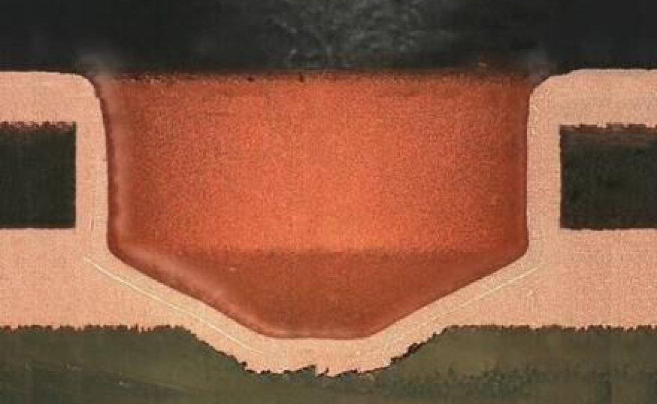
But if the blind buried holes are all on the same layer, they cannot be pressed together at once. As shown in the figure below, layers 1-3 and 6-8 are blind holes, while layers 3-6 are buried holes. So both the fifth and sixth layers have blind buried holes. At this point, laser drilling is needed. The steps are as follows:
Step 1: Layer 3-6 and produce copper wire and PTH as standard 2-layer PCB;
Step 2: Press the 2nd to 7th layers together, and laser drill the 2nd to 3rd, 6th, and 7-XNUMX layers to produce copper wire and electroplate through holes;
Step 3: Layering 1-8 layers and laser drilling 1-2, 7, 8-XNUMX layers to produce copper wire on the outer layer, and plating through holes.
This method is very popular, and now almost all blind buried hole PCB manufacturing industries around the world are using this method. Many large blind buried hole PCB manufacturers can achieve this.
This method of making blind buried hole plates is an extension of the above sequential lamination/drilling (Method B), but the difference is that it is added layer by layer from the inside to the outside of the plate. Usually, it starts from the second layer of the middle PCB and uses laser drilled blind holes to connect all additional layers. These through holes in blind buried PCB are stacked micro through holes or staggered micro through holes. Stacking through holes means that the through holes are located exactly at the top of another layer of through holes, but staggered through holes are not. This type of blind buried hole PCB is called an arbitrary layer PCB. There are three methods for drilling any layer:
Photo Definition Type
In the process of blind buried hole PCB production, a photosensitive resistor and a permanent dielectric layer are first applied to the board at the same time, then aligned with a specific position, exposed and developed with a negative film, exposing the bottom copper pad to form a bowl shaped blind hole of the blind buried hole board. Then, chemical copper and copper plating are thoroughly added to etch the outer layer of the circuit and blind hole on the blind buried hole PCB, and the outer layer of the circuit and blind hole can be etched, or conductivity can be achieved without copper plating. Copper paste or silver paste can also be filled. Of course, in the process of blind buried hole PCB production, other layers can be added using the same method.
Plasma etching:
This is a patent of a company, so they named their business name after the demonstration method.
Laser ablation:
In the HDI PCB manufacturing process, there are mainly three types: commonly used CO2 lasers, excimer lasers, and Nd: YAG lasers.
Laser drilling technology for blind hole machining has the advantages of high precision, strong universality, high efficiency, low cost, and significant comprehensive technical and economic benefits. Currently, it has become one of the key technologies in the field of modern blind hole PCB manufacturing. Before the emergence of lasers, only high hardness materials could be used to drill holes on lower hardness materials, making drilling on high hardness diamonds a complex task. After the emergence of lasers, this type of drilling became fast and safe in blind buried hole PCB manufacturing. However, the holes drilled by laser are conical instead of cylindrical like mechanical drilling, which is very inconvenient in some places of blind buried orifice plates. Programmable control of graphic output through galvanometer.
Laser drilling is the process of focusing a laser into a high-intensity heat source, heating the material to be drilled, melting or vaporizing the material within the laser action area, and then evaporating to form holes. The laser beam is highly concentrated in space and time, and using lens focusing can reduce the spot diameter to a laser power density of 5 ^ 10 to 15 ^ 10 w/cm2. Such high power density can be used for laser drilling on almost any material.
Laser drill, as a type of blind hole in HDI PCB, has its characteristics in PCB manufacturing:
A. Under normal circumstances, any layer of copper can be electroplated onto a single pattern plate in one go.
B. In general, after the lamination process, if the board thickness is greater than or equal to 80MIL, the through-hole board will need to be electroplated with a whole board pattern. Therefore, in PCB manufacturing, blind hole electroplating cannot be done on the outer layer.
C. After meeting the above conditions, blind hole electroplating requires the following operations:
If the line width of the outer layer is greater than 6MIL and the thickness of the PTH board is less than 80MIL, then the entire board can be electroplated during the blind hole electroplating process.
When the outer line width is greater than 6MIL, but the PTH plate thickness is greater than 80MIL, during blind hole electroplating, the outer layer should be coated with a film on the surface to protect it.
The outer wiring width is less than 6MIL. At the same time, the thickness of the PTH board is greater than or equal to 80MIL. During blind hole electroplating, the outer layer needs to be coated with a film on the surface to protect it.
If pursuing cost-effective FPC manufacturing services, choosing a Chinese manufacturer is the best choice. As a manufacturing powerhouse, China has abundant resources, cheap labor, and a large number of technical personnel. We recommend Haibo, a Chinese FPC assembly service provider with over 10 years of experience, who has performed outstandingly in various aspects
Efficient and reasonable quotation:There is an efficient quotation process to assist you in making decisions, providing reasonable prices and highly competitive quotes in China.
High quality and reliable products:Produce high standard printed circuit boards, manufacture and test according to specifications, international standards, and internal controls, and conduct pre production inspections to ensure robust processes.
Quick and on-time delivery:The assembly equipment is in good condition, with high productivity, minimal downtime, short delivery time, and also provides urgent services.
Timely and effective response:Always respond to customer needs, provide accurate information, answer questions through multiple channels, and offer one-stop services.
Strong technical strength:China's FPC manufacturing technology is leading, and Haibo has a complete SMT solution that covers assembly, inspection, and other capabilities. It also provides prototype production and customization services.
mobile phone: 86-15113315665
Contact: Chen Changhai
mobile phone: 86-18676922028
E-mall: haibo_fpcba1668@163.com
Address: 3rd Floor, Building 2, Fuxing Industrial Park, Building B, Chuangye 1st Road, Jiangbian Community, Songgang Street, Bao'an District, Shenzhen