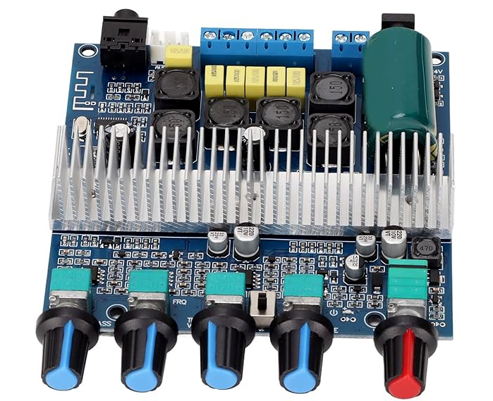
All components in the amplifier PCB are selected at the schematic level and must be placed on the PCB according to the layout guidelines.
Layout considerations also start with the application of PCB amplifiers, as some applications (such as theaters and heavy-duty speaker equipment) require 6 or more PCB layers.
Most amplifiers adopt a four layer stacked structure. The top layer is usually the signal layer, the second and third layers are the ground layers, and the bottom layer is a mixed layer of the signal layer and the power layer.
The decoupler must be placed near the pins. The minimum capacitance value and packaging size must be placed near the IC power pins.
The wiring path must be sufficient to carry power, and the via cannot be located between pins or critical signal lines.
The amplifier design consists of primary and secondary side pins. The primary and secondary pins are powered by different power sources.
The power pin and ground pin are connected using star grounding technology.
The other two types of capacitors are crucial for signal design in PCB amplifier circuits, namely switch capacitors and pump capacitors. This can achieve soft switching of signals without generating switching noise that affects adjacent signals or power lines.
Charge pump capacitors must have small parasitic capacitance and low inductance. Among these design styles, it is best to use high line density to minimize parasitic noise to the greatest extent possible.
The D-class output signal needs to be sent in two layers of PCB, with a minimum trace width of 30 mil and an output trace width of at least 60 mil.
Your trusted partner and one-stop supplier for FPC/PCB manufacturing, component procurement, FPC/PCB assembly, and electronic manufacturing. With over 16 years of experience, we have been providing high-quality FPC/PCB at competitive prices to over 1000 customers worldwide. Our company has passed ISO9001:2015 certification and UL certification, and all of our products have undergone 100% electronic testing and passed AOI and X-RAY inspections to meet the highest industry standards. Therefore, please obtain an immediate quote from our sales team as we will handle the remaining matters.
Haibo is an expert in the field of FPC/PCB manufacturing and surface mount assembly in China. Since our establishment in 2017, we have been providing high-quality PCBs to over 1000 customers worldwide. Our factory has passed ISO14001, ISO9001:2015, TS16949, and ISO13485:2016 certifications. We are one of the most trusted small and medium-sized FPC/PCB manufacturers in China.