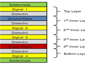
A layer stack is an arrangement of dielectric layers and copper layers. Now, among the 6 copper layers, 4 layers are sandwiched between 5 dielectric layers for insulation, which may be core boards or pre impregnated materials (6 layers of PCB can have more than 1 core board), and there are also 2 layers for placing components. Some layer stacks are as follows:
SIG-GND–PWR–PWR-GND–SIG
This type of layer stack is called a symmetric layer stack. This stack is used to manage high-speed signals, as high-speed signals require a ground plane as a reference plane. Components that use high-speed signals typically use two different voltages, so having two independent power layers is very convenient. The use of reference layers at the top and bottom levels allows the use of vias to transmit high-speed signals (although it is never recommended to use vias to transmit high-speed signals).
This type of stack is very common in network switches, where most network switch ICs consume different voltages and require impedance controlled wiring to transmit high-frequency signals.
SIG- GND – PWR – GND – SIG – GND
This type of layer stack is called an asymmetric layer stack. This layer stack may have less wiring space than other layer stacks, but due to its excellent ground shielding, its EMC performance is also outstanding. Please note that all signal and power layers have adjacent ground planes, which provide high EMC and high power integrity for the stack.
If the signal you are processing is very sensitive to EMI, the internal signal layer will be completely sandwiched by the ground layer. To improve EMC in this stack, you may consider using multiple cores (which would increase the cost of 6 layers of PCB). But there is an obvious problem with the stack, as the bottom layer is a ground layer, it may be difficult to effectively place components at the bottom layer, so only the top layer is suitable for placing components.
SIG – PWR – SIG – SIG – GND – SIG
This is one of the most basic layer stacks, and it is also the most likely layer stack to occur after spontaneously changing layers from 4 to 6. Although this layer stack may look tempting due to the abundance of available signal layers, its EMC performance is very poor, and due to poor shielding, it can be considered to have poor layer utilization. This layer stack may only be suitable for PCBs used in pure DC applications or extremely low-speed signal applications.
SIG – GND – PWR – SIG – GND – SIG
This layer stack is an improved version of the previous layer stack. The top and bottom layers of this stack both have a ground reference plane. This stack can be used for high-speed signals with higher IO counts. Suggest using this stack instead of the previous one for better EMC.
The selection of layer stacks is not limited to the above content. You can create a stack based on your understanding of the requirements. Many 6-layer PCB manufacturers offer layer stacks that are much cheaper than custom layer stacks.
Your trusted partner and one-stop supplier for FPC/PCB manufacturing, component procurement, FPC/PCB assembly, and electronic manufacturing. With over 16 years of experience, we have been providing high-quality FPC/PCB at competitive prices to over 1000 customers worldwide. Our company has passed ISO9001:2015 certification and UL certification, and all of our products have undergone 100% electronic testing and passed AOI and X-RAY inspections to meet the highest industry standards. Therefore, please obtain an immediate quote from our sales team as we will handle the remaining matters.
Haibo is an expert in the field of FPC/PCB manufacturing and surface mount assembly in China. Since our establishment in 2017, we have been providing high-quality PCBs to over 1000 customers worldwide. Our factory has passed ISO14001, ISO9001:2015, TS16949, and ISO13485:2016 certifications. We are one of the most trusted small and medium-sized FPC/PCB manufacturers in China.