Technology
Acceptance criteria for PCBA
Side bracket, flip and component end bending

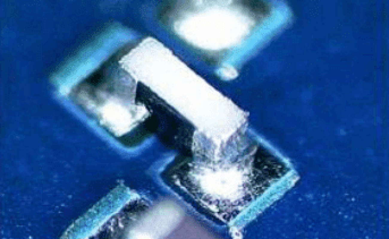
The following figure shows the defect: the ratio of width (W) to height (H) is greater than 2:1; The number of weldable end faces (metal cover ends) of the component is less than 3.
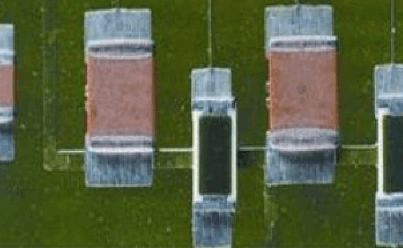
The following figure shows the defect: the material surface of the SMD component is exposed, with electrical materials piled up and installed on the circuit board of the PCB. This should be a process warning.
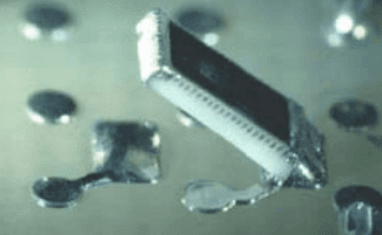
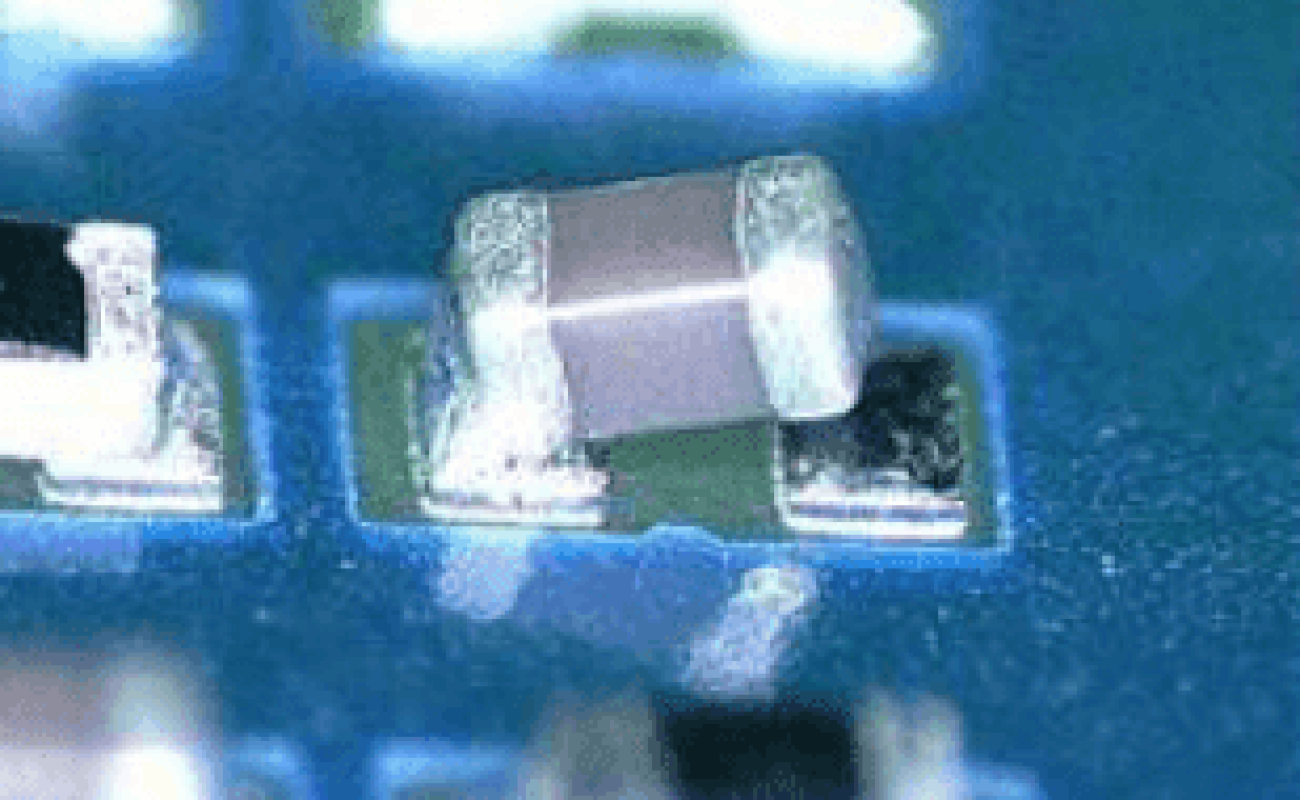
The following figure shows the defect: distortion at the end of the SMD component.
The ratio of width to height shall not exceed 2:1. The surface of the solder pad and the solderable end of the component are completely 100% wetted and in overlapping contact. The component has 3 or more solderable ends and good wetting properties on the vertical surface.
Attach the SMD component material surface without exposed electrical material accumulation onto the PCB surface.
End warping of SMD components (known as Tomstoning).
  • What is the IPC-A-610 standardWhat is the IPC-A-610 standard
  • What PCB assembly acceptance standards do we follow in Haibo?What PCB assembly acceptance standards do we follow in Haibo?
  • What are the main differences between IPC-A-610 Level 2 and Level 3What are the main differences between IPC-A-610 Level 2 and Level 3
  • Detailed Explanation of Visual Acceptance Standards for PCB AssemblyDetailed Explanation of Visual Acceptance Standards for PCB Assembly
  • Less soldering amount, more soldering amountLess soldering amount, more soldering amount
  • Offset of castle shaped components, width and height of weldable endsOffset of castle shaped components, width and height of weldable ends
  • Get a Quotation
    Your trusted partner and one-stop supplier for FPC/PCB manufacturing, component procurement, FPC/PCB assembly, and electronic manufacturing. With over 16 years of experience, we have been providing high-quality FPC/PCB at competitive prices to over 1000 customers worldwide. Our company has passed ISO9001:2015 certification and UL certification, and all of our products have undergone 100% electronic testing and passed AOI and X-RAY inspections to meet the highest industry standards. Therefore, please obtain an immediate quote from our sales team as we will handle the remaining matters.
    Haibo is an expert in the field of FPC/PCB manufacturing and surface mount assembly in China. Since our establishment in 2017, we have been providing high-quality PCBs to over 1000 customers worldwide. Our factory has passed ISO14001, ISO9001:2015, TS16949, and ISO13485:2016 certifications. We are one of the most trusted small and medium-sized FPC/PCB manufacturers in China.
    Contact Us

    mobile phone: 86-15113315665

    Contact: Chen Changhai

    mobile phone: 86-18676922028

    E-mall: haibo_fpcba1668@163.com

    Address: 3rd Floor, Building 2, Fuxing Industrial Park, Building B, Chuangye 1st Road, Jiangbian Community, Songgang Street, Bao'an District, Shenzhen

    Copyright © Shenzhen Haibo Precision Circuit Co., Ltd. All rights reservedGuangdong ICP No. 2022143581