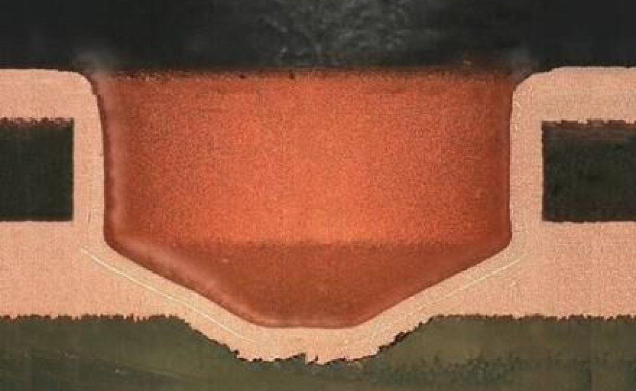
A. Under normal circumstances, any layer of copper can be electroplated onto a single pattern plate in one go.
B. In general, after the lamination process, if the board thickness is greater than or equal to 80MIL, the through-hole board will need to be electroplated with a whole board pattern. Therefore, in PCB manufacturing, blind hole electroplating cannot be done on the outer layer.
C. After meeting the above conditions, blind hole electroplating requires the following operations:
If the line width of the outer layer is greater than 6MIL and the thickness of the PTH board is less than 80MIL, then the entire board can be electroplated during the blind hole electroplating process.
When the outer line width is greater than 6MIL, but the PTH plate thickness is greater than 80MIL, during blind hole electroplating, the outer layer should be coated with a film on the surface to protect it.
The outer wiring width is less than 6MIL. At the same time, the thickness of the PTH board is greater than or equal to 80MIL. During blind hole electroplating, the outer layer needs to be coated with a film on the surface to protect it.
mobile phone: 86-15113315665
Contact: Chen Changhai
mobile phone: 86-18676922028
E-mall: haibo_fpcba1668@163.com
Address: 3rd Floor, Building 2, Fuxing Industrial Park, Building B, Chuangye 1st Road, Jiangbian Community, Songgang Street, Bao'an District, Shenzhen