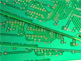
Double sided PCB manufacturing involves executing various steps in a serial manner to produce high-quality double-sided printed circuit boards:
1. Circuit design
Double sided PCB manufacturers can use various software to design circuits, which are used to draw schematic and layout designs for PCB boards. In the case of double-sided PCB, circuit design is accomplished by forming copper traces on two layers (top and bottom). The Gerber files for layout design will be generated through PCB software and used to print the required circuits on a double-sided PCB board.
2. Basic material preparation
The dielectric material of double-sided printed circuit boards is usually made of FR4 resin. This FR4 resin is composed of a grid of glass frames woven together. This glass structure is combined with resin to form a material called prepreg. FR4 dielectric material and copper foil are attached to both sides of the substrate material through heat treatment and cut into the required blocks for production, typically 18 x 24 inches.
3. Circuit printing
The process of printing the required circuit on copper foil is called photolithography. During this process, a photosensitive material is used to cover the copper foil, and then the required circuit is engraved in the form of a photomask. Using ultraviolet light, it will pass through this photomask layer and project onto the copper foil. Through this process, the desired circuit pattern will be formed on the PCB.
4. Copper wire etching
During this process, the exposed copper will be immersed in etching chemicals, and under the action of these chemicals, the photosensitive material will remove all the exposed copper, leaving behind the copper wire required for the circuit.
5. Drilling
In order to form mounting holes and vias on the PCB, it is necessary to use a drilling machine to generate holes of various diameters on the PCB. Installation holes are non plated through holes, while vias are plated through holes filled with copper to create electrical connections.
6. Solder mask printing
During this process, both sides of the PCB will be coated with a polymer protective layer, usually green. This layer of PCB can prevent copper wire corrosion and also protect the circuit board from environmental factors such as dust, smoke, and moisture. It can also prevent the formation of solder bridges during component installation.
7. Silk screen printing
During this process, white ink is used to generate symbols for indicators and components to be soldered onto the PCB. This screen printing process can also be used to print any type of desired logo.
8. Surface treatment
For copper areas not covered by solder mask, we need to cover them with a thick layer of metal to prevent oxidation. In addition, this helps with the soldering of components on the PCB.
9. Quality testing and inspection
After the PCB is completed, thorough testing and inspection are always required, such as open and short circuit testing, AOI inspection, visual inspection, solderability testing, intermediate section and inspection.
Your trusted partner and one-stop supplier for FPC/PCB manufacturing, component procurement, FPC/PCB assembly, and electronic manufacturing. With over 16 years of experience, we have been providing high-quality FPC/PCB at competitive prices to over 1000 customers worldwide. Our company has passed ISO9001:2015 certification and UL certification, and all of our products have undergone 100% electronic testing and passed AOI and X-RAY inspections to meet the highest industry standards. Therefore, please obtain an immediate quote from our sales team as we will handle the remaining matters.
Haibo is an expert in the field of FPC/PCB manufacturing and surface mount assembly in China. Since our establishment in 2017, we have been providing high-quality PCBs to over 1000 customers worldwide. Our factory has passed ISO14001, ISO9001:2015, TS16949, and ISO13485:2016 certifications. We are one of the most trusted small and medium-sized FPC/PCB manufacturers in China.