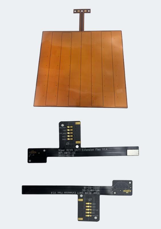
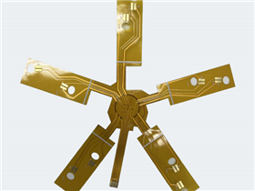
Choose suitable substrates, such as polyimide (PI) or polyester (PET) films, which have good flexibility and heat resistance. Covering the surface of the substrate with a layer of copper foil, the thickness of the copper foil is usually between 12 μ m and 35 μ m, depending on the current demand and design requirements.
Line production
Transfer circuit patterns onto copper foil using photolithography. Firstly, a layer of photoresist material is coated on the copper foil, and then the circuit pattern is exposed onto the photoresist layer through a photomask. Etch the exposed copper foil to form the desired circuit pattern. Etching accuracy is crucial for the performance of circuit boards.
Layering and Drilling
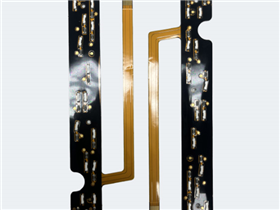
For multi-layer FPCs or FPCs that require interlayer connections, they need to be laminated together through a lamination process. Process through holes using laser drilling or mechanical drilling to achieve electrical connections between layers.
Electroplating and surface treatment
Perform electroplating treatment on the drilled through holes to ensure electrical connection between layers. Surface treatment of FPC to improve soldering performance and oxidation resistance. Common surface treatment processes include chemical gold plating, silver plating, or organic solder mask (OSP) treatment.
Forming and cutting
Cover the circuit layer with an insulating film to protect the circuit and prevent short circuits and external damage. Separate the finished product from the entire substrate using methods such as punching or laser cutting, and cut it into a shape that meets the design requirements.
Testing and Inspection
Conduct strict electrical performance testing, bending testing, tensile strength testing, etc. on FPC to ensure that the conductivity, solderability, and structural integrity of the circuit meet the design requirements.
Your trusted partner and one-stop supplier for FPC/PCB manufacturing, component procurement, FPC/PCB assembly, and electronic manufacturing. With over 16 years of experience, we have been providing high-quality FPC/PCB at competitive prices to over 1000 customers worldwide. Our company has passed ISO9001:2015 certification and UL certification, and all of our products have undergone 100% electronic testing and passed AOI and X-RAY inspections to meet the highest industry standards. Therefore, please obtain an immediate quote from our sales team as we will handle the remaining matters.
Haibo is an expert in the field of FPC/PCB manufacturing and surface mount assembly in China. Since our establishment in 2017, we have been providing high-quality PCBs to over 1000 customers worldwide. Our factory has passed ISO14001, ISO9001:2015, TS16949, and ISO13485:2016 certifications. We are one of the most trusted small and medium-sized FPC/PCB manufacturers in China.