After generating the design schematic and layout, send the Gerber file containing layer stacking information and other manufacturing instructions to the rigid flexible PCB manufacturer for rigid flexible PCB manufacturing. The following is an overview of different rigid flexible PCB manufacturing processes.
Layering: The flexible layer is laminated together with the rigid part through adhesive bonding, heating, and pressure. The flexible circuit is composed of polyimide core, adhesive, and copper film, while the rigid part is composed of FR4 substrate, copper, and solder mask layer. PCB flexible and rigid materials must be strictly bonded according to specifications.
Drilling: The drilling process can be completed by mechanical or laser drill bits. The received Gerber file is used as a reference for hole positions. Drilling is usually the slowest process in the entire rigid flexible PCB production line. It is very important to minimize drilling burrs during the drilling process. Clean burrs and debris using standard methods.
Copper plating: Drills (also known as "vias") are plated with copper to provide electrical connections across layers.
Etching: During the etching process, copper traces that do not belong to the circuit layout will be removed from the substrate. The etching process is completed through photolithography technology, in which a mask pattern is used to expose and develop photosensitive materials and etch away unwanted copper surfaces.
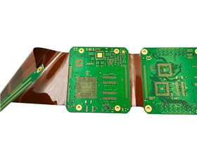
Solder mask: The green coating you typically see on a PCB is a product of the solder mask process. The solder mask layer on the PCB serves not only as a protective layer, but also as an isolation layer and insulation layer. It isolates conductive pads to avoid short circuits between adjacent pads.
Surface treatment: Apply a protective layer on the copper pad to provide a solderable contact pad and protect the copper from oxidation. The most common surface treatment techniques include electroless nickel immersion (ENIG), organic surface protection (OSP), and hot air solder leveling (HASL).
Screen printing: A layer of screen printing that displays reference marks, manufacturing and assembly instructions, traceability, and other information is printed on a rigid flexible printed circuit board. This can be achieved through photolithography, where photosensitive materials are used to create patterns, or through direct laser printing.
Electrical testing: Electrical testing is conducted in the later stages of the rigid flexible PCB manufacturing process to ensure that only defect free products can be delivered to customers. The latest testing technology makes it possible to automatically test the continuity of circuits using Pogo needle fixtures.
Your trusted partner and one-stop supplier for FPC/PCB manufacturing, component procurement, FPC/PCB assembly, and electronic manufacturing. With over 16 years of experience, we have been providing high-quality FPC/PCB at competitive prices to over 1000 customers worldwide. Our company has passed ISO9001:2015 certification and UL certification, and all of our products have undergone 100% electronic testing and passed AOI and X-RAY inspections to meet the highest industry standards. Therefore, please obtain an immediate quote from our sales team as we will handle the remaining matters.
Haibo is an expert in the field of FPC/PCB manufacturing and surface mount assembly in China. Since our establishment in 2017, we have been providing high-quality PCBs to over 1000 customers worldwide. Our factory has passed ISO14001, ISO9001:2015, TS16949, and ISO13485:2016 certifications. We are one of the most trusted small and medium-sized FPC/PCB manufacturers in China.