A typical LED PCB design involves steps such as design preparation, schematic design, Gerber and BOM design, and material selection. When designing, we use CAD software, which will help us obtain the schematic and related Gerber and BOM files for LED PCB manufacturing. We need to follow these principles in the design of LED PCB circuit boards.
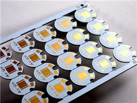
Correct material selection: We will consider factors such as dielectric properties, thermal conductivity, strength, etc. to choose suitable substrate materials. Commonly used materials include aluminum or copper substrates.
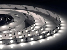
Thermal management: LED PCB adopts various thermal management technologies, such as MCPCB with thermal conductive substrate and thermal vias (specifically designed for heat transfer) and PCB with metal back (for better cooling).
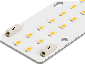
Electrical Layout: In LED PCBs, they have complex electrical layouts designed to enhance the power supply and control of LEDs. The design of copper wire can handle high current, reduce voltage drop, and provide continuous illumination for LED arrays.
Optical design: In order to shape and guide the light emitted by LEDs, PCB LEDs integrate some optical components. Optical components such as reflectors, lenses, and diffusers play an important role in achieving ideal effects such as beam angle, uniformity, and color mixing.
Component installation: PCB LEDs can accommodate different types of LEDs, including surface mount and through-hole packaging. The placement of LEDs must be precise, therefore automatic picking and placing machines are used to ensure good alignment and better welding accuracy.
Your trusted partner and one-stop supplier for FPC/PCB manufacturing, component procurement, FPC/PCB assembly, and electronic manufacturing. With over 16 years of experience, we have been providing high-quality FPC/PCB at competitive prices to over 1000 customers worldwide. Our company has passed ISO9001:2015 certification and UL certification, and all of our products have undergone 100% electronic testing and passed AOI and X-RAY inspections to meet the highest industry standards. Therefore, please obtain an immediate quote from our sales team as we will handle the remaining matters.
Haibo is an expert in the field of FPC/PCB manufacturing and surface mount assembly in China. Since our establishment in 2017, we have been providing high-quality PCBs to over 1000 customers worldwide. Our factory has passed ISO14001, ISO9001:2015, TS16949, and ISO13485:2016 certifications. We are one of the most trusted small and medium-sized FPC/PCB manufacturers in China.